 Professional high frequency circuit board supplier

Ajinomoto Package Substrate Manufacturer
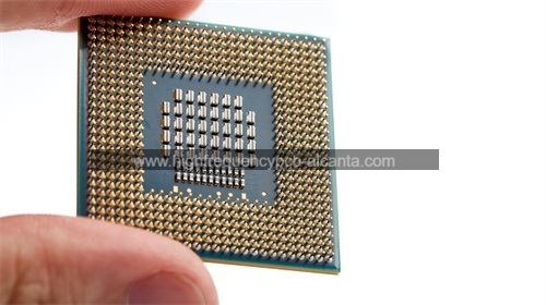
Ajinomoto Package Substrate Manufacturer,Ajinomoto Package Substrate is an advanced organic packaging substrate manufactured using high-performance compound materials. It features excellent thermal stability and electrical performance, making it particularly suitable for high-density and complex circuit layouts. Ajinomoto Package Substrate achieves precise dimensional control and supports various packaging and chip integration technologies such as BGA and CSP through advanced manufacturing processes and multilayered designs. Widely applied in semiconductor packaging, communication equipment, and consumer electronics, it provides critical packaging solutions and reliability for modern electronic devices.
What is Ajinomoto Package Substrate?
Ajinomoto Package Substrate refers to a type of semiconductor packaging substrate produced by Ajinomoto Fine-Techno Co., Inc., a leading company in the field of electronic materials and substrates. These substrates are crucial components in semiconductor packaging, providing a foundation for mounting and interconnecting semiconductor devices within electronic products.
Key features of Ajinomoto Package Substrates include their high thermal conductivity, excellent electrical properties, and reliability under varying operational conditions. They are designed to efficiently dissipate heat generated by semiconductor devices, thereby enhancing overall performance and longevity.
Ajinomoto offers various types of package substrates tailored to different applications and industry requirements. These substrates play a critical role in modern electronics, ensuring the integrity and functionality of semiconductor devices in demanding environments such as automotive, telecommunications, and consumer electronics.
The manufacturing process involves advanced techniques to achieve precise dimensions, fine pitch interconnections, and optimal thermal management. Ajinomoto’s expertise in material science and semiconductor packaging enables them to provide solutions that meet the stringent performance and reliability standards demanded by the semiconductor industry.
In summary, Ajinomoto Package Substrates represent cutting-edge technology in semiconductor packaging, supporting the development of faster, more efficient, and reliable electronic devices across various sectors globally.
Ajinomoto Package Substrate Manufacturer
What are Ajinomoto Package Substrate Design Guidelines?
Design guidelines for Ajinomoto Package Substrates are essential to ensure optimal performance and reliability in semiconductor packaging. While specific guidelines may vary based on the substrate type and application, here are some general aspects typically covered:
- Dimensional Specifications: Guidelines specify the exact dimensions, including thickness, width, and length of the substrate. These dimensions are critical to ensure compatibility with the semiconductor devices and the overall assembly process.
- Material Selection:Recommendations on the choice of substrate materials are provided to meet thermal management, electrical performance, and mechanical strength requirements. Ajinomoto substrates often use materials with high thermal conductivity and good electrical properties to ensure efficient heat dissipation and signal integrity.
- Layer Configuration:Guidelines detail the layer stack configuration, including the number and types of metal layers, dielectric layers, and any additional features like embedded components or heat sinks. This ensures that the substrate can support the required electrical interconnections and thermal management.
- Routing and Via Design: Guidelines cover routing considerations such as trace widths, spacing, and via design rules. These ensure signal integrity, minimize crosstalk, and provide sufficient electrical connectivity between semiconductor devices and other components on the substrate.
- Thermal Management: Recommendations for thermal vias, thermal pads, and heat spreaders are provided to manage heat dissipation effectively. This is crucial for maintaining semiconductor device reliability and performance under varying operational conditions.
- Electrical Performance: Guidelines ensure that the substrate meets electrical performance requirements, including impedance control, signal integrity, and power distribution characteristics. This is achieved through careful design of trace geometries and material selection.
- Reliability Considerations: Guidelines address reliability aspects such as mechanical stress, thermal cycling, and moisture resistance. Design features like proper solder mask application, pad design, and substrate material properties are optimized to enhance long-term reliability.
- Manufacturability: Design guidelines also consider manufacturability aspects such as panelization, fiducial placement, and alignment features. These ensure that the substrate can be manufactured efficiently with minimal defects and within cost-effective parameters.
By adhering to these design guidelines, engineers can ensure that Ajinomoto Package Substrates perform optimally in various electronic applications, meeting stringent performance, reliability, and manufacturability requirements of the semiconductor industry.
What is the Ajinomoto Package Substrate Fabrication Process?
The fabrication process of Ajinomoto Package Substrates involves several specialized steps to create high-performance semiconductor packaging substrates. Here’s a general overview of the typical fabrication process:
- Substrate Material Selection: The process begins with selecting high-quality substrate materials that meet specific requirements for thermal conductivity, electrical properties, and mechanical strength. Ajinomoto typically uses materials like ceramic or organic substrates depending on the application.
- Substrate Preparation: The selected substrate materials undergo preparation steps such as cleaning and surface treatment to ensure proper adhesion and uniformity for subsequent layers and components.
- Layer Deposition: The fabrication process involves depositing various layers onto the substrate. This includes metal layers (typically copper) for electrical interconnections and possibly other layers for specific functionalities such as barrier layers or solder resist.
- Photolithography: Photolithography is used to define the pattern of conductive traces and other features on the substrate. A photoresist layer is applied, exposed to UV light through a mask, developed, and then etched to create the desired circuit pattern.
- Plating: Metal layers are often plated onto the substrate to build up the conductive traces and vias. This step may include electroplating or other deposition techniques to ensure precise thickness and conductivity.
- Dielectric Layer Deposition: Dielectric layers are deposited over the metal traces to insulate them and provide mechanical support. These layers also contribute to the overall electrical performance and reliability of the substrate.
- Via Formation: Vias are created to establish electrical connections between different layers of the substrate. Techniques such as laser drilling or mechanical drilling followed by chemical or plasma etching are used to form vias through the substrate layers.
- Surface Finishing:The substrate surface is finished with coatings such as solder mask and surface finishes (e.g., ENIG – Electroless Nickel Immersion Gold) to protect exposed metal traces, facilitate soldering, and enhance reliability.
- Testing and Inspection: Throughout the fabrication process, rigorous testing and inspection are conducted to ensure quality and adherence to design specifications. This includes electrical testing, dimensional inspection, and reliability testing under simulated operational conditions.
- Final Assembly: Depending on the specific application, the completed substrates may undergo final assembly processes where semiconductor devices, heat sinks, or other components are attached using advanced packaging techniques.
- Quality Control: Quality control measures are implemented at each stage of fabrication to identify and rectify any defects or deviations from specifications, ensuring that the finished Ajinomoto Package Substrates meet high industry standards for performance and reliability.
By meticulously following these fabrication processes, Ajinomoto produces package substrates that are crucial components in modern semiconductor devices, offering high thermal conductivity, electrical performance, and reliability across diverse electronic applications.
How do you manufacture Ajinomoto Package Substrates?
Manufacturing Ajinomoto Package Substrates involves a series of specialized processes aimed at producing high-quality semiconductor packaging substrates. Here’s a structured overview of the typical manufacturing process:
- Substrate Material Selection: Begin by selecting substrate materials suited to the application’s thermal conductivity, electrical properties, and mechanical strength requirements. Ajinomoto uses ceramic or organic substrates based on specific needs.
- Substrate Preparation: Prepare the chosen substrate materials through cleaning and surface treatments to ensure uniformity and optimal adhesion for subsequent layers and components.
- Layer Deposition: Deposit various layers onto the substrate. This includes metal layers (often copper) for electrical interconnections, along with potential additional layers like barrier coatings or solder resist for specific functionalities.
- Photolithography: Utilize photolithography to define precise patterns of conductive traces and other features on the substrate. Apply a photoresist layer, expose it to UV light through a mask, develop it, and etch it to create the desired circuit pattern.
- Plating: Plate metal layers onto the substrate to build up conductive traces and vias. Techniques such as electroplating ensure the correct thickness and conductivity for each layer.
- Dielectric Layer Deposition: Deposit dielectric layers over the metal traces to insulate them and provide structural support. These layers enhance electrical performance and substrate reliability.
- Via Formation: Form vias to establish electrical connections between different substrate layers. Methods like laser drilling or mechanical drilling followed by chemical or plasma etching create vias through the substrate layers.
- Surface Finishing: Apply coatings such as solder mask and surface finishes (e.g., ENIG) to protect exposed metal traces, facilitate soldering, and improve overall substrate reliability.
- Testing and Inspection: Conduct rigorous testing and inspection throughout the manufacturing process to verify adherence to design specifications. This includes electrical testing, dimensional checks, and reliability testing under simulated operational conditions.
- Final Assembly: Depending on the application, complete substrates may undergo final assembly processes. These include attaching semiconductor devices, heat sinks, or other components using advanced packaging techniques.
- Quality Control: Implement stringent quality control measures at every stage to detect and rectify defects or deviations. Ensure that finished Ajinomoto Package Substrates meet industry standards for performance, reliability, and durability.
By meticulously following these manufacturing processes, Ajinomoto produces package substrates that play essential roles in modern semiconductor devices. These substrates offer high thermal conductivity, excellent electrical properties, and robust performance across a wide range of electronic applications.
How much should Ajinomoto Package Substrates cost?
The cost of Ajinomoto Package Substrates can vary significantly based on several factors:
- Substrate Material: The type of substrate material used (ceramic or organic) affects the cost. Ceramic substrates, known for their high thermal conductivity and reliability, tend to be more expensive than organic substrates.
- Complexity and Design: The complexity of the substrate design, including the number of layers, size, and intricacy of the circuit patterns, influences the cost. More complex designs with finer features and tighter tolerances generally incur higher manufacturing costs.
- Volume and Production Scale: Economies of scale apply in substrate manufacturing. Larger production volumes typically result in lower per-unit costs due to optimized manufacturing processes and bulk material purchasing.
- Additional Features:Specialized features such as embedded components, advanced surface finishes (e.g., gold plating), and specific thermal management solutions can add to the substrate’s cost.
- Quality and Reliability Requirements: Meeting stringent quality and reliability standards through extensive testing and quality control measures may increase overall production costs.
- Market Conditions: Supply chain dynamics, market demand, and fluctuations in raw material prices can also impact substrate costs.
To obtain specific pricing for Ajinomoto Package Substrates, it’s recommended to directly contact Ajinomoto Fine-Techno Co., Inc. or their authorized distributors. They can provide tailored pricing based on your specific requirements, volume commitments, and customization needs.
What is Ajinomoto Package Substrate base material?
Ajinomoto Package Substrates utilize various base materials depending on the specific requirements of the application. Typically, these substrates can be categorized into two main types based on the base material used:
- Ceramic Substrates: Ajinomoto manufactures ceramic-based package substrates, which are known for their excellent thermal conductivity, mechanical strength, and reliability. Ceramic substrates are often composed of materials such as alumina (Al2O3) or aluminum nitride (AlN). These materials provide high thermal conductivity to efficiently dissipate heat generated by semiconductor devices, making them suitable for applications requiring robust thermal management.
- Organic Substrates: Ajinomoto also produces organic-based package substrates. Organic substrates are typically made from materials such as epoxy resin or polyimide. They offer advantages such as lower cost, lighter weight, and flexibility in design compared to ceramic substrates. Organic substrates are commonly used in applications where cost-effectiveness and specific electrical performance requirements are prioritized.
The choice between ceramic and organic substrates depends on factors such as thermal management needs, electrical performance requirements, mechanical durability, and overall cost considerations for the specific electronic application. Ajinomoto Fine-Techno Co., Inc. tailors their substrate offerings to meet these diverse needs in the semiconductor packaging industry.
Which companies manufacture Ajinomoto Package Substrates?
Ajinomoto Package Substrates (味の素封装基板) are manufactured by Ajinomoto Fine-Techno Co., Inc., based in Tokyo, Japan. Ajinomoto Fine-Techno is a leading company specializing in electronic materials and packaging technologies, with extensive experience and technical expertise in the field of electronic packaging. They provide various high-performance package substrate solutions to the global electronics industry.
The manufacturing of Ajinomoto Package Substrates involves advanced materials science and precise manufacturing processes. Key manufacturing steps include material selection, layer stacking, photolithography, plating, via formation, surface treatment, testing, and quality control. Their products typically use ceramic or organic materials as substrate bases to meet thermal management, electrical performance, and reliability requirements for different applications.
As a company with advanced manufacturing equipment and a skilled technical team, we are also capable of producing similar package substrate products. We emphasize technological innovation and quality control, adhering to a customer-first approach to provide customized solutions. With our professional R&D and production teams, we deliver high-performance, reliable electronic package substrate products tailored to meet specific customer needs.
In the increasingly competitive electronic industry landscape, we continuously introduce advanced production technologies and management practices to ensure product quality and delivery efficiency. We are committed to collaborating with leading global supply chain partners to secure raw material supply and cost control, thereby offering competitive pricing and stable product supply.
In summary, as a company with technological strength and market experience, we have the confidence and capability to manufacture and supply products similar to Ajinomoto Package Substrates. We provide critical packaging solutions for electronic products, helping our customers succeed in the competitive market.
What are the 7 qualities of good customer service?
The seven qualities of good customer service typically include:
- Responsiveness: Good customer service involves promptly addressing customer inquiries, concerns, or issues. This responsiveness shows customers that their needs are valued and attended to promptly.
- Empathy: Showing empathy means understanding and acknowledging the customer’s emotions and concerns. It involves listening actively and responding in a compassionate manner.
- Patience: Patience is crucial in customer service interactions, especially when dealing with challenging situations or customers. It involves remaining calm, composed, and respectful, even in difficult circumstances.
- Knowledgeability: Good customer service representatives possess adequate knowledge about the products or services they offer. They are able to provide accurate information and guidance to customers, enhancing their confidence and trust.
- Clarity: Communication clarity ensures that information and instructions are conveyed clearly and understandably to customers. This helps prevent misunderstandings and promotes effective resolution of issues.
- Professionalism: Professionalism in customer service involves maintaining a positive attitude, being courteous, and adhering to company policies and standards. It builds trust and confidence in the customer-company relationship.
- 7. Problem-Solving Skills: Effective problem-solving skills enable customer service representatives to resolve issues efficiently and effectively. They can identify root causes, explore solutions, and follow through to ensure customer satisfaction.
These qualities collectively contribute to creating positive customer experiences, fostering loyalty, and enhancing the reputation of the company for excellent customer service.
FAQs about Ajinomoto Package Substrates
What are Ajinomoto Package Substrates?
Ajinomoto Package Substrates are specialized materials used in semiconductor packaging. They provide a foundation for mounting and interconnecting semiconductor devices within electronic products.
What types of materials are used in Ajinomoto Package Substrates?
Ajinomoto uses ceramic and organic materials for their package substrates. Ceramic substrates offer high thermal conductivity and reliability, while organic substrates provide flexibility and cost-effectiveness.
What are the advantages of Ajinomoto Package Substrates?
Advantages include high thermal conductivity, excellent electrical properties, and reliability under various operational conditions. They enhance the performance and longevity of semiconductor devices.
What industries use Ajinomoto Package Substrates?
These substrates are used in various industries such as automotive electronics, telecommunications, consumer electronics, and industrial applications where high-performance electronic packaging is required.
How are Ajinomoto Package Substrates manufactured?
The manufacturing process involves steps like material selection, layer deposition, photolithography, via formation, surface finishing, testing, and quality control to ensure high-quality, reliable substrates.
What customization options are available for Ajinomoto Package Substrates?
Ajinomoto offers customization options based on specific customer requirements, including substrate material, dimensions, layer configurations, and additional features like embedded components or specialized coatings.
Where can I purchase Ajinomoto Package Substrates?
Ajinomoto Fine-Techno Co., Inc. typically supplies their package substrates through authorized distributors or directly, catering to global electronics manufacturers and suppliers.
What are the environmental and regulatory considerations of Ajinomoto Package Substrates?
Ajinomoto adheres to environmental regulations and standards in the production and disposal of their substrates, ensuring compliance with international environmental guidelines.