 Professional high frequency circuit board supplier
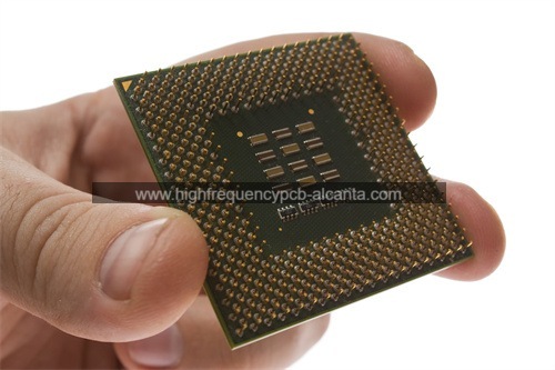
What is WLP Package Substrate?
WLP Package Substrate Manufacturer,WLP (Wafer-Level Package) substrate revolutionizes semiconductor packaging by integrating chips at the wafer level, streamlining manufacturing and enhancing performance. WLP substrates offer compact designs, directly connecting chips through solder bumps, reducing interconnect length, and improving signal integrity. They ensure efficient heat dissipation, mechanical stability, and reliable electrical connections, critical for high-density applications. Widely utilized in mobile devices, IoT, and consumer electronics, WLP package substrates support miniaturization and enhance system performance. Their precise construction and advanced materials enable the development of smaller, lighter, and more efficient electronic devices, meeting the demands of modern technology.
WLP stands for Wafer-Level Packaging, which refers to a technology in semiconductor packaging where the integrated circuits (ICs) are assembled and packaged at the wafer level, rather than being diced into individual chips first. The WLP process typically involves packaging multiple ICs simultaneously on a wafer, followed by singulation (dicing) to separate the individual packaged chips.
The package substrate in WLP refers to the material on which the ICs are mounted and interconnected. It serves as the foundation for the electrical connections between the ICs and the external circuitry. The choice of substrate material depends on various factors such as electrical performance, thermal management, cost, and form factor requirements.
Some common materials used for WLP package substrates include organic substrates (such as laminates or build-up substrates), silicon interposers, and glass interposers. Each of these materials offers different advantages and trade-offs in terms of performance, cost, and integration capabilities.
Overall, WLP with its package substrate plays a crucial role in enabling the miniaturization, performance optimization, and cost reduction of semiconductor devices, making it a key technology in the advancement of integrated circuits and electronic devices.
WLP Package Substrate Manufacturer
What are the functions of WLP Package Substrate?
The functions of WLP package substrate include the following aspects:
Mechanical support and protection: The package substrate provides a sturdy support platform for the integrated circuits to prevent mechanical damage and the effects of external environments.
Electrical connection: Circuitry and solder points on the package substrate provide electrical connections, enabling signal transmission and data exchange between the ICs and external circuits (e.g., PCBs).
Thermal management: Through proper layout and material selection, the package substrate can effectively disperse and conduct the heat generated by integrated circuits, helping to maintain the ICs’ operating temperature within a safe range.
Signal transmission and integration: Wires and solder points on the package substrate allow signal transmission and data exchange between different ICs, enabling the integration and collaboration of multiple ICs.
Electromagnetic compatibility (EMC): By designing and laying out circuits to reduce electromagnetic interference (EMI) and providing grounding and shielding, the package substrate can help ensure that electronic devices comply with electromagnetic compatibility standards.
Overall, the WLP package substrate plays a crucial role in protection, connection, thermal management, signal transmission, and EMC, making it an indispensable component in integrated circuit systems.
What are the different types of WLP Package Substrate?
There are several different types of WLP (Wafer-Level Packaging) package substrates, each with its own characteristics and advantages. Some common types include:
Organic Substrates: These are typically made of organic materials such as laminates or build-up substrates. Organic substrates offer good electrical performance, cost-effectiveness, and flexibility in design. They are widely used in various applications due to their ease of manufacturing and compatibility with standard semiconductor processes.
Silicon Interposers: Silicon interposers are made of silicon wafers with through-silicon vias (TSVs) that provide vertical interconnects between different layers of the package. Silicon interposers offer high density, high bandwidth, and excellent thermal performance, making them suitable for high-performance applications such as high-speed computing and networking.
Glass Interposers: Glass interposers use glass as the substrate material, with embedded copper traces for electrical interconnections. Glass interposers offer advantages such as low loss, high bandwidth, and compatibility with high-temperature processing. They are often used in radio frequency (RF) and millimeter-wave applications where signal integrity and thermal performance are critical.
Ceramic Substrates: Ceramic substrates, such as alumina (Al2O3) or aluminum nitride (AlN), offer excellent thermal conductivity and mechanical stability. They are suitable for applications requiring high power dissipation and reliability, such as power amplifiers, RF modules, and high-power LED packages.
Wafer-Level Chip-Scale Packages (WLCSP): While not strictly a substrate type, WLCSP is a type of WLP where the package substrate is the silicon wafer itself. In WLCSP, the IC is directly attached to the wafer surface, and the package is formed directly on the wafer without the need for additional substrates. WLCSP offers a compact form factor, high electrical performance, and cost-effectiveness for applications requiring small-sized packages.
These are some of the common types of WLP package substrates, each offering different benefits and suitable for various applications based on performance, cost, and form factor requirements.
What is the relationship between WLP Package Substrate and IC packaging?
The relationship between WLP (Wafer-Level Packaging) package substrate and IC (Integrated Circuit) packaging is that the package substrate serves as the foundation for assembling and interconnecting the integrated circuits within the package. In other words, the package substrate is an integral part of the overall IC packaging process.
Here’s how the package substrate relates to IC packaging:
Foundation for IC Mounting: The ICs are mounted onto the package substrate, where they are positioned and secured in place. The substrate provides a stable platform for the ICs during the packaging process.
Interconnection: The package substrate contains the wiring and interconnects necessary for connecting the ICs to each other and to external circuitry. This includes wire bonding, flip-chip bonding, or other interconnection methods used to establish electrical connections between the ICs and the substrate.
Thermal Management: The package substrate plays a role in dissipating heat generated by the integrated circuits. It may include features such as thermal vias or heat spreaders to enhance thermal conductivity and heat dissipation, thereby helping to maintain the ICs within their safe operating temperature range.
Protection: The package substrate provides mechanical support and protection for the integrated circuits against physical damage, moisture, and other environmental factors. It helps to encapsulate and shield the ICs from external elements, ensuring their reliability and longevity.
Integration: The package substrate facilitates the integration of multiple ICs into a single package. By providing the necessary electrical and mechanical infrastructure, the substrate enables the assembly of complex IC packages containing multiple chips, sensors, and other components.
Overall, the package substrate is a critical component of IC packaging, serving as the platform for mounting, interconnecting, and protecting the integrated circuits within the package. Its design and characteristics directly impact the performance, reliability, and form factor of the packaged ICs.
How does WLP Package Substrate differ from PCB?
WLP (Wafer-Level Packaging) package substrate and PCB (Printed Circuit Board) are both essential components in electronic devices, but they serve different purposes and have distinct characteristics. Here are some key differences between WLP package substrate and PCB:
Function:
WLP Package Substrate: The primary function of the WLP package substrate is to provide a foundation for mounting and interconnecting integrated circuits (ICs) within a semiconductor package. It is specifically designed for packaging and connecting ICs at the wafer level.
PCB: A PCB serves as a platform for mounting and interconnecting various electronic components, including ICs, resistors, capacitors, and connectors. It provides electrical connections between components and mechanical support for the entire electronic system.
Scale:
WLP Package Substrate: WLP package substrates are typically smaller in size compared to PCBs. They are designed to accommodate the dimensions of individual ICs and are optimized for miniaturization, allowing for high-density packaging of ICs.
PCB: PCBs can vary widely in size, ranging from small boards used in consumer electronics to large boards used in industrial equipment or servers. They are designed to support multiple components and provide space for routing complex electrical connections.
Manufacturing Process:
WLP Package Substrate: WLP package substrates are manufactured using semiconductor fabrication processes. These processes involve advanced lithography, etching, deposition, and metallization techniques performed on semiconductor wafers.
PCB: PCBs are manufactured using printed circuit board fabrication processes. This typically involves printing conductive traces and insulating layers onto a substrate material (such as fiberglass-reinforced epoxy), followed by drilling, plating, and soldering of components.
Integration:
WLP Package Substrate: WLP package substrates are integrated directly into semiconductor packages, forming an integral part of the IC packaging process. They are specifically designed to meet the requirements of individual ICs and optimize electrical performance, thermal management, and reliability.
PCB: PCBs serve as standalone platforms that can accommodate various types of electronic components from different manufacturers. They are designed to support the integration of diverse components and enable the assembly of complex electronic systems.
In summary, while both WLP package substrate and PCB play crucial roles in electronic devices, they differ in terms of function, scale, manufacturing process, and integration. WLP package substrates are specialized components designed for packaging and connecting ICs at the wafer level, while PCBs are general-purpose platforms used to support the integration of various electronic components in electronic systems.
What are the structure and production technology of WLP Package Substrate?
The structure and production technology of WLP (Wafer-Level Packaging) package substrate can vary depending on the specific design requirements and the choice of substrate material. However, here is a general overview of the structure and production technology of WLP package substrate:
Structure:
The structure of a typical WLP package substrate may include the following components:
Substrate Material: The substrate material serves as the base on which the integrated circuits (ICs) are mounted and interconnected. Common substrate materials include organic substrates (e.g., laminates or build-up substrates), silicon interposers, glass interposers, or ceramic substrates.
Interconnects: The substrate contains conductive traces, vias, and solder pads that provide electrical connections between the ICs and external circuitry. These interconnects may be formed using various techniques such as metal deposition, etching, plating, and soldering.
Passive Components (optional): In some cases, passive components such as resistors, capacitors, or inductors may be integrated directly onto the substrate to save space and simplify assembly.
Thermal Management Features (optional): The substrate may include features such as thermal vias, heat spreaders, or thermal interface materials to improve heat dissipation and thermal management for the ICs.
Production Technology:
The production technology for WLP package substrate typically involves the following steps:
Substrate Fabrication: The substrate material is prepared and processed to form the base substrate. This may involve cutting, laminating, or stacking layers of material, depending on the substrate type.
Surface Preparation: The surface of the substrate is prepared for subsequent processing steps, such as cleaning, planarization, and surface treatment to enhance adhesion and solderability.
Circuit Patterning: Conductive traces, vias, and solder pads are patterned onto the substrate using techniques such as photolithography, etching, or printing.
Metallization: The patterned features are metallized to create electrical connections and solderable surfaces. This may involve processes such as metal deposition, plating, or sputtering.
Passive Component Integration (if applicable): Passive components may be integrated onto the substrate using surface mount technology (SMT) or other assembly techniques.
Thermal Management Feature Integration (if applicable): Thermal management features such as thermal vias or heat spreaders may be incorporated into the substrate design and fabricated using specialized processes.
Final Inspection and Testing: The finished substrates undergo inspection and testing to ensure quality and reliability before they are assembled into semiconductor packages.
Overall, the production technology for WLP package substrate involves a combination of materials processing, patterning, metallization, and integration techniques tailored to meet the specific requirements of IC packaging.
Frequently Asked Questions (FAQs)
What is WLP package substrate?
WLP package substrate is a component used in semiconductor packaging technology to mount and interconnect integrated circuits (ICs) at the wafer level. It provides a foundation for packaging multiple ICs simultaneously before singulation (dicing) into individual chips.
What are the advantages of WLP package substrate?
WLP package substrates offer several advantages, including miniaturization, improved electrical performance, enhanced thermal management, increased integration density, and cost-effectiveness compared to traditional packaging methods.
What are the different types of WLP package substrates?
Common types of WLP package substrates include organic substrates (e.g., laminates or build-up substrates), silicon interposers, glass interposers, and ceramic substrates. Each type has its own characteristics and suitability for various applications.
How are WLP package substrates manufactured?
The manufacturing process for WLP package substrates involves substrate fabrication, surface preparation, circuit patterning, metallization, integration of passive components (if applicable), integration of thermal management features (if applicable), and final inspection and testing.
What factors should be considered when selecting a WLP package substrate?
Factors to consider when selecting a WLP package substrate include electrical performance, thermal management capabilities, integration density, reliability, cost, and compatibility with specific semiconductor processes and applications.
What are the applications of WLP package substrates?
WLP package substrates are used in various applications such as mobile devices, consumer electronics, automotive electronics, medical devices, networking equipment, and high-performance computing systems where miniaturization, high density, and reliability are critical.
How does WLP package substrate differ from PCB?
WLP package substrate is specifically designed for mounting and interconnecting ICs at the wafer level, whereas PCB (Printed Circuit Board) serves as a platform for mounting and interconnecting various electronic components in electronic systems.
What are the trends and developments in WLP package substrate technology?
Recent trends in WLP package substrate technology include advancements in materials and manufacturing processes, increased integration density, improved thermal management techniques, and the development of innovative packaging solutions to meet the demands of emerging applications such as 5G, artificial intelligence (AI), and Internet of Things (IoT).
Conclusion
Microtrace Substrate