 Professional high frequency circuit board supplier

Wire Bonding Chip Scale Package Substrates Manufacturer
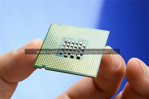
Wire Bonding Chip Scale Package Substrates Manufacturer,Wire Bonding Chip Scale Package (CSP) Substrates are specialized platforms used in the assembly of semiconductor devices. These substrates provide the necessary framework for connecting the die to the external circuitry through wire bonding, a process where fine wires are used to connect the semiconductor chip to the substrate. CSP substrates are designed to be extremely compact, enabling significant miniaturization of electronic components. They offer excellent thermal and electrical performance, ensuring reliable operation of the device. Widely used in applications such as smartphones, tablets, and other high-density electronics, Wire Bonding CSP Substrates are essential for achieving higher functionality in smaller form factors.
What is Wire Bonding Chip Scale Package Substrates?
Wire Bonding Chip Scale Package (CSP) substrates are specialized components used in semiconductor packaging, specifically designed to facilitate the connection of a semiconductor die to the external circuitry through wire bonding techniques. These substrates are crucial in the miniaturization and efficient performance of electronic devices.
A Chip Scale Package (CSP) is a type of integrated circuit (IC) package that is only slightly larger than the size of the die itself, typically no more than 1.2 times its original dimensions. This compact size offers several advantages, such as reduced footprint, enhanced electrical performance, and improved thermal management. CSPs are widely used in applications where space and weight are critical factors, including mobile devices, wearables, and IoT (Internet of Things) devices.
Wire bonding, one of the primary methods for creating electrical connections between the semiconductor die and the package, involves the use of fine wires (usually made of gold, aluminum, or copper) to establish connections. The wires are bonded to the die’s pads and the corresponding pads on the substrate. This technique is favored for its reliability, cost-effectiveness, and the ability to handle high-frequency signals.
The substrates used in wire bonding CSPs are designed to provide mechanical support and electrical interconnections. They are typically made from materials such as BT (Bismaleimide-Triazine) resin, FR-4 (Flame Retardant 4), or ceramic, chosen for their excellent thermal and electrical properties. These materials ensure the substrate can withstand the rigors of wire bonding processes and the operational environment of the final device.
In summary, Wire Bonding Chip Scale Package Substrates are essential components in modern electronics, enabling the compact and efficient packaging of semiconductor devices. Their design and material selection are critical to ensuring reliable performance, making them a key element in the advancement of miniaturized electronic technologies.
Wire Bonding Chip Scale Package Substrates Manufacturer
What are the Wire Bonding Chip Scale Package Substrates Design Guidelines?
When designing Wire Bonding Chip Scale Package (CSP) substrates, several key guidelines must be followed to ensure optimal performance, reliability, and manufacturability. Here are the primary design considerations:
- Die Size and Pad Layout: The substrate design must accommodate the exact dimensions of the chip while providing sufficient space for wire bonding. Pad layout should be precise, with adequate spacing between bond pads to prevent short circuits and ensure reliable wire bonding.
- Bond Pad Design: Bond pads on the substrate should be sized and positioned to match the chip’s bond pads. The pad’s surface finish must support effective wire bonding, typically involving gold, nickel, or other compatible materials.
- Wire Bonding Area: Ensure that the area around the bond pads is free from obstructions that could interfere with the wire bonding process. The substrate must provide a flat and clean surface for the wire bonds.
- Thermal Management: Proper thermal dissipation is critical to prevent overheating. The substrate design should incorporate heat sinks or thermal vias to manage heat generated by the chip. Thermal conductivity of the substrate material plays a crucial role in heat dissipation.
- Electrical Performance: The substrate must support high-frequency signals with minimal signal loss and interference. This requires careful consideration of trace widths, spacing, and the dielectric properties of the substrate material.
- Mechanical Stability: The substrate should be robust enough to support the chip and wire bonds throughout the device’s lifecycle. This includes resistance to mechanical stress and vibration.
- Material Selection: Choose substrate materials that offer the right balance of electrical performance, thermal conductivity, and mechanical strength. Common materials include BT resin, FR-4, and various ceramics.
- Manufacturability: Design the substrate for ease of manufacturing and assembly. This includes considerations for etching processes, adhesive bonding, and compatibility with automated assembly systems.
- Reliability Testing: Incorporate design features that facilitate reliability testing, such as thermal cycling and humidity testing, to ensure the substrate can withstand harsh environmental conditions.
- Cost Efficiency: Optimize the design to balance performance and cost. Considerations include material costs, manufacturing processes, and assembly complexity.
By adhering to these design guidelines, engineers can ensure that Wire Bonding Chip Scale Package Substrates meet the necessary performance and reliability standards for modern electronic devices.
What is the Wire Bonding Chip Scale Package Substrates Fabrication Process?
The fabrication process for Wire Bonding Chip Scale Package (CSP) substrates involves several key steps to create a reliable and high-performance substrate for semiconductor devices. Here’s an overview of the typical fabrication process:
- Substrate Material Preparation: The process begins with selecting and preparing the substrate material, which can be BT (Bismaleimide-Triazine) resin, FR-4 (Flame Retardant 4), or ceramic. The material is cut to the desired size and shape.
- Layer Formation: For substrates with multiple layers, the next step is to form these layers. This involves lamination, where sheets of substrate material are bonded together using heat and pressure. This creates a stack of layers that will be patterned to form the final substrate structure.
- Photoresist Application: A photoresist layer is applied to the substrate surface. This light-sensitive material will define the areas to be etched away or left intact. The photoresist is typically applied using spin coating.
- Patterning: The photoresist-coated substrate is exposed to ultraviolet (UV) light through a photomask that defines the desired pattern of traces and pads. The exposed photoresist is then developed to reveal the pattern that will be etched into the substrate.
- Etching: The exposed areas of the substrate are etched away using chemical etchants or plasma etching, creating the necessary traces, pads, and vias. This step defines the electrical pathways and bond pads on the substrate.
- Deposition of Metal Layers: Thin metal layers, such as copper, gold, or nickel, are deposited onto the substrate using techniques like sputtering or electroplating. These metals form the electrical traces, bond pads, and other conductive features necessary for wire bonding.
- Photoresist Removal: The remaining photoresist is stripped away, leaving behind the patterned metal layers on the substrate.
- Via Formation: Vias, or vertical interconnects, are created by drilling or etching holes through the substrate layers. These vias are then filled with metal to establish electrical connections between different layers of the substrate.
- Solder Mask Application: A solder mask is applied to protect the metal traces and bond pads from soldering and environmental damage. The solder mask also defines the areas where solder will be applied.
- Final Testing and Inspection:The fabricated substrate undergoes rigorous testing and inspection to ensure it meets design specifications and quality standards. This includes checking for electrical continuity, mechanical integrity, and adherence to design rules.
- Dicing and Packaging: The completed substrates are diced into individual units, each ready for chip mounting and wire bonding. The substrates are then packaged and prepared for integration into electronic devices.
The Wire Bonding Chip Scale Package Substrates fabrication process combines precision engineering and advanced materials science to produce high-performance substrates suited for compact and efficient semiconductor packaging.
How Do You Manufacture Wire Bonding Chip Scale Package Substrates?
Manufacturing Wire Bonding Chip Scale Package (CSP) substrates involves a series of precise and controlled steps to ensure the production of high-quality substrates. Here’s a detailed overview of the typical manufacturing process:
- Material Selection and Preparation: Begin by selecting the appropriate substrate material, such as BT (Bismaleimide-Triazine) resin, FR-4 (Flame Retardant 4), or ceramic. The material is cut into the required shapes and sizes for substrate panels or sheets.
- Layer Lamination: For multilayer substrates, layers of the substrate material are laminated together using heat and pressure. This process creates a stack of layers, each of which will be patterned and processed to form the final substrate structure.
- Photoresist Application: A layer of photoresist, a light-sensitive material, is applied to the surface of the substrate. This is typically done using spin coating, which ensures a uniform thickness of photoresist across the substrate.
- Exposure and Patterning: The photoresist-coated substrate is exposed to ultraviolet (UV) light through a photomask, which defines the pattern for the electrical traces, bond pads, and vias. The photoresist is then developed, revealing the areas that will be etched away or remain.
- Etching: The exposed substrate is subjected to etching processes, which can be chemical or plasma-based. This removes unwanted material and creates the necessary features, such as traces and pads, according to the pattern defined by the photoresist.
- Metal Deposition: Thin metal layers, such as copper, gold, or nickel, are deposited onto the substrate using techniques like sputtering, evaporation, or electroplating. These metal layers form the conductive paths and bond pads required for wire bonding.
- Photoresist Stripping: After metal deposition, the remaining photoresist is removed using a chemical solvent or other stripping methods, leaving the patterned metal features intact on the substrate.
- Via Formation: Vias are created by drilling or etching holes through the substrate layers. These holes are then filled with metal to establish electrical connections between different layers of the substrate.
- Solder Mask Application: A solder mask is applied to protect the metal traces and bond pads from damage during soldering and handling. The solder mask also defines where solder will be applied during assembly.
- Final Inspection and Testing: The substrate undergoes comprehensive inspection and testing to ensure it meets design specifications. This includes checking electrical continuity, mechanical integrity, and adherence to quality standards.
- Dicing and Packaging: The completed substrates are diced into individual units, ready for chip mounting and wire bonding. Each substrate is then packaged and prepared for integration into electronic devices.
- Wire Bonding: In the final assembly phase, semiconductor chips are mounted onto the CSP substrates, and wire bonding is performed to establish electrical connections between the chip and the substrate’s bond pads.
Each of these steps requires precise control and high-quality materials to ensure the performance and reliability of the Wire Bonding Chip Scale Package Substrates, making them suitable for advanced electronic applications.
How Much Should Wire Bonding Chip Scale Package Substrates Cost?
The cost of Wire Bonding Chip Scale Package (CSP) substrates can vary widely based on several factors, including:
- Substrate Material: The choice of material (e.g., BT resin, FR-4, ceramic) influences cost. Advanced materials with better thermal and electrical properties are generally more expensive.
- Complexity and Layer Count: More complex designs with multiple layers or intricate patterns increase manufacturing complexity and cost. Higher layer counts and more intricate designs require additional processing steps and quality control.
- Size and Dimensions: The size of the CSP substrates affects the cost. Larger substrates or those with specific dimensions may cost more due to material usage and processing requirements.
- Quantity and Production Volume: Larger production volumes often reduce the per-unit cost due to economies of scale. Low-volume or prototype runs generally have higher per-unit costs.
- Manufacturing Technology: The specific technologies and processes used in fabrication (e.g., advanced etching techniques, precision metal deposition) impact costs. More advanced technologies can increase the price.
- Customization and Specifications: Custom features or specifications, such as unique bond pad layouts or specialized thermal management solutions, can add to the cost.
- Quality and Testing: Substrates that undergo rigorous testing and quality assurance processes will generally cost more due to the added steps in the manufacturing process.
- Supplier and Market Conditions: Prices can vary based on the supplier and current market conditions, including demand for substrates and availability of raw materials.
As a rough estimate, Wire Bonding CSP substrates can range from a few dollars to over $50 per unit, depending on the factors mentioned. For high-volume production or less complex designs, costs can be on the lower end, while specialized or low-volume substrates with advanced features may be on the higher end. For a precise cost estimate, it’s best to request quotes from manufacturers based on your specific requirements and production volume.
What is Wire Bonding Chip Scale Package Substrates Base Material?
Wire Bonding Chip Scale Package (CSP) substrates are typically made from base materials that provide a suitable balance of electrical, thermal, and mechanical properties. The choice of base material is crucial for ensuring the substrate’s performance and reliability. Common base materials used for CSP substrates include:
- BT (Bismaleimide-Triazine) Resin:BT resin is a popular choice for CSP substrates due to its excellent thermal stability, good electrical insulation properties, and low dielectric constant. It provides a reliable platform for high-density interconnections and is well-suited for applications requiring robust performance under thermal stress.
- FR-4 (Flame Retardant 4): FR-4 is a widely used fiberglass-reinforced epoxy resin that offers good mechanical strength, moderate thermal performance, and cost-effectiveness. It is often used in applications where high performance is not as critical, but where a reliable and economical material is needed.
- Ceramic: Ceramic substrates are chosen for their superior thermal conductivity, high electrical insulation, and mechanical stability. They are used in high-power and high-frequency applications where enhanced thermal management and electrical performance are required.
- Polyimide:Polyimide materials are known for their high thermal stability and electrical insulation properties. They are often used in applications where high temperatures and stringent performance requirements are present.
- PTFE (Polytetrafluoroethylene): PTFE substrates are used in applications requiring very low dielectric constants and excellent chemical resistance. They are typically used in high-frequency or microwave applications.
- High-Density Interconnect (HDI) Materials: HDI materials are designed for very fine-pitch designs and provide enhanced electrical performance and thermal management. These materials often incorporate advanced laminates and resins to support complex, high-density designs.
The choice of base material depends on the specific requirements of the application, including electrical performance, thermal management, mechanical strength, and cost considerations. Each material has its strengths and trade-offs, and the selection is typically guided by the desired performance characteristics and application needs.
Which Company Makes Wire Bonding Chip Scale Package Substrates?
Many companies specialize in producing Wire Bonding Chip Scale Package (CSP) substrates, offering a variety of solutions to meet different electronic application needs. Here are some well-known manufacturers and suppliers:
- AdvanTech: AdvanTech is a leading electronics component manufacturer offering a range of CSP substrate solutions widely used in communication, consumer electronics, and automotive fields. Their substrates are known for high quality and reliability, suitable for various high-performance applications.
- NXP Semiconductors: NXP Semiconductors is a globally recognized semiconductor company, with CSP substrate products that excel in automotive electronics and industrial applications. They offer various types of substrates, including advanced solutions for high-frequency applications.
- ASE Group: ASE Group is one of the world’s largest semiconductor packaging and testing companies, providing a range of packaging solutions, including CSP substrates. Their products are widely used in consumer electronics, communications, and computing sectors.
- TSMC (Taiwan Semiconductor Manufacturing Company): TSMC, a leading global foundry, also offers CSP substrate solutions. Their CSP substrates are known for high precision and performance, used in various high-tech products.
- Kyocera: Kyocera offers various ceramic substrate solutions, including CSP substrates. Their ceramic substrates are renowned for excellent thermal conductivity and electrical performance, suitable for high-power and high-frequency applications.
Our company also manufactures Wire Bonding Chip Scale Package (CSP) substrates. As a company specializing in advanced PCB technology, we possess the equipment and expertise required for CSP substrate production. We can provide a range of CSP substrates to meet different customer needs. Our products include substrates for high-frequency applications, precise connections, and high-performance electronic devices. By using high-quality base materials and advanced manufacturing processes, we ensure that each CSP substrate meets industry standards for performance and reliability.
Our manufacturing process includes material selection, lamination, patterning, metal deposition, and final testing and inspection to ensure each substrate meets high-quality requirements. We also offer customization services to support various complex application scenarios. Our goal is to provide customers with efficient, reliable, and up-to-date CSP substrate solutions to help them succeed in the electronics industry.
What are the 7 Qualities of Good Customer Service?
Good customer service is essential for building and maintaining strong relationships with customers. Here are seven key qualities that define excellent customer service:
- Responsiveness: Good customer service is characterized by prompt and efficient responses to customer inquiries and issues. This means addressing questions and concerns quickly, whether through phone, email, or chat, and providing timely updates.
- Empathy: Empathetic customer service representatives understand and share the feelings of their customers. They listen actively, acknowledge customers’ emotions, and show genuine concern for their problems, which helps in building trust and rapport.
- Knowledgeability:Representatives should have a deep understanding of the products or services offered, as well as company policies and procedures. Being knowledgeable allows them to provide accurate information, solve problems effectively, and guide customers to the best solutions.
- Courtesy: Politeness and professionalism are crucial in customer service. Representatives should use respectful language, maintain a positive attitude, and treat customers with dignity, regardless of the situation.
- Problem-Solving Skills: Effective customer service involves finding solutions to customer issues efficiently. Representatives should be resourceful, creative, and proactive in resolving problems, ensuring that customers are satisfied with the outcome.
- Clear Communication: Communication should be clear and straightforward, avoiding jargon and technical terms that may confuse customers. Good customer service involves explaining things in a way that customers can easily understand and ensuring that all information is conveyed accurately.
- Consistency: Consistent service quality is important for maintaining customer trust. This means providing the same high level of service across all interactions, whether customers contact the company through different channels or at different times.
Incorporating these qualities into customer service practices helps create positive experiences, fosters customer loyalty, and contributes to a strong reputation for the company.
FAQs about Wire Bonding Chip Scale Package Substrates
What are Wire Bonding Chip Scale Package (CSP) Substrates?
Wire Bonding CSP substrates are components used in semiconductor packaging that allow for the connection of a semiconductor die to external circuitry via wire bonding. They are compact, offering a footprint close to the size of the die itself.
What materials are used for CSP substrates?
Common materials include BT (Bismaleimide-Triazine) resin, FR-4 (Flame Retardant 4), ceramic, and polyimide. The choice depends on the specific application requirements, including electrical performance, thermal management, and cost.
What are the advantages of CSP substrates?
CSP substrates offer several advantages, such as a smaller footprint compared to other package types, reduced electrical and thermal resistance, and improved performance in high-frequency applications.
How are CSP substrates manufactured?
The manufacturing process involves material preparation, layering, photoresist application, patterning, etching, metal deposition, via formation, solder mask application, and final testing. Each step is crucial for creating a reliable and high-performance substrate.
What applications are CSP substrates used in?
CSP substrates are used in various electronic devices, including mobile phones, tablets, wearables, and other compact and high-performance electronics where space is limited and performance is critical.
What are the key design considerations for CSP substrates?
Design considerations include die size and pad layout, bond pad design, thermal management, electrical performance, mechanical stability, material selection, manufacturability, reliability testing, and cost efficiency.
How do you choose the right CSP substrate for a project?
Choosing the right CSP substrate involves evaluating the specific requirements of your application, such as electrical and thermal performance needs, space constraints, and budget. Consulting with manufacturers and testing prototypes can help in making an informed decisio