 Professional high frequency circuit board supplier

Ultra Thin Multilayer BGA Substrates Manufacturer
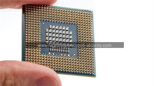
Ultra Thin Multilayer BGA Substrates Manufacturer,Ultra Thin Multilayer BGA (Ball Grid Array) substrates are highly sophisticated components used in advanced semiconductor packaging. These substrates feature multiple layers of interconnects within an exceptionally thin form factor, enabling high-density integration and efficient signal routing. Typically made from advanced materials like BT resin or high-performance organic laminates, they offer excellent electrical performance, thermal stability, and mechanical strength. The ultra-thin design helps reduce the overall package height, making them ideal for compact electronic devices such as smartphones, tablets, and wearable technology. These substrates support high-speed data transfer and robust performance, meeting the demands of modern, high-performance electronics.
What is Ultra Thin Multilayer BGA Substrates?
Ultra Thin Multilayer BGA Substrates are critical components used in integrated circuit packaging, particularly for high-density, high-performance electronic products. Ball Grid Array (BGA) packaging is a technique that connects chips to substrates using spherical solder joints to form electrical connections. Ultra Thin Multilayer BGA Substrates take this packaging technology further by employing a multilayer structure and ultra-thin materials. This design allows for more electrical connections and more complex circuit designs while maintaining a lightweight and thin physical profile.
These substrates typically use high-performance materials such as ceramics, BT resin, or high-density polymers to ensure stability and reliability in high-frequency and high-temperature environments. The ultra-thin design makes them particularly suitable for compact electronic devices like smartphones, tablets, and portable gaming consoles, where space and weight are critical considerations. Moreover, the ultra-thin multilayer structure permits more electrical layers, supporting more complex circuits and higher data transfer rates.
Due to the complex manufacturing process and the need for high precision, producing Ultra Thin Multilayer BGA Substrates requires advanced technology and equipment. The manufacturing process involves precise lamination, micro-fabrication, and stringent quality control to ensure high performance and reliability in practical applications. Therefore, Ultra Thin Multilayer BGA Substrates play a crucial role in modern electronic products and are an indispensable part of high-performance electronic devices.
Ultra Thin Multilayer BGA Substrates Manufacturer
What are the Ultra Thin Multilayer BGA Substrates Design Guidelines?
- Layer Count and Thickness: When designing Ultra Thin Multilayer BGA Substrates, carefully determine the number of layers needed for your circuit. The ultra-thin design requires precise control of layer thickness to ensure structural integrity and performance. Typically, layer thicknesses range from 0.1 mm to 0.3 mm, depending on the specific requirements of the application.
- Material Selection: Choose high-quality materials that offer excellent electrical performance and mechanical stability. Common materials include advanced ceramics, BT resin, and high-density polymers. Ensure that the chosen materials can withstand the operating conditions, such as high frequencies and temperatures.
- Thermal Management: Effective thermal management is crucial for ultra-thin substrates due to the high density of components and potential heat generation. Incorporate thermal vias, heat spreaders, and other cooling mechanisms to dissipate heat efficiently and prevent overheating.
- Signal Integrity:Maintain signal integrity by designing controlled impedance lines and minimizing signal crosstalk. Use proper trace routing techniques and ensure that the substrate layout supports high-speed signal transmission without introducing interference.
- Mechanical Stability:Despite the thin profile, ensure that the substrate maintains adequate mechanical stability. Use reinforcement techniques such as stiffeners or additional layers where necessary to prevent warping or bending that could affect performance.
- Manufacturing Tolerances: Adhere to tight manufacturing tolerances to ensure high precision in the production of ultra-thin multilayer substrates. This includes maintaining accurate layer alignment, hole dimensions, and trace widths.
- Testing and Quality Control: Implement rigorous testing and quality control procedures to detect any defects or issues in the substrate. This includes electrical testing, visual inspections, and mechanical stress tests to ensure the substrate meets the required performance standards.
- Design for Manufacturability: Design the substrate with manufacturability in mind. Simplify the design where possible to reduce production complexity and costs. Consider factors such as ease of lamination, drilling, and etching during the design phase.
By following these design guidelines, you can create ultra-thin multilayer BGA substrates that offer high performance, reliability, and efficiency in advanced electronic applications.
What is the Ultra Thin Multilayer BGA Substrates Fabrication Process?
The fabrication of ultra-thin multilayer BGA (Ball Grid Array) substrates involves a series of precise and intricate steps to ensure high performance and reliability. Here’s an overview of the fabrication process:
- Material Preparation: Start with high-quality base materials, such as ceramics, BT resin, or high-density polymers. These materials must meet stringent performance criteria for dielectric properties, thermal conductivity, and mechanical strength.
- Lamination:Stack multiple layers of the substrate material according to the design specifications. Use a lamination process involving heat and pressure to bond these layers together, creating a multilayer stack. The precision of lamination affects the overall thickness and alignment of the substrate.
- Photolithography: Apply a photosensitive layer (photoresist) on the substrate. Using photolithography, expose the photoresist to UV light through a mask that defines the circuit patterns. Develop the exposed photoresist to reveal the desired circuit patterns on the substrate.
- Etching: Use chemical etching to remove unwanted copper or other conductive material from the substrate, following the patterns defined by the photolithography process. This step creates the circuit traces and pads.
- Drilling: Drill precise holes (vias) through the substrate layers to create electrical connections between them. The drilling must be highly accurate to ensure reliable interlayer connections and maintain the substrate’s thin profile.
- Plating: Plate the drilled vias with a conductive material, such as copper, to establish electrical connections between different layers of the substrate. This step also includes applying a thin layer of copper on the surface for additional circuitry.
- Inspection and Testing: Conduct rigorous inspection and testing of the substrate to ensure that it meets design specifications and quality standards. This includes checking for defects, verifying electrical connectivity, and assessing mechanical integrity.
- Solder Mask and Surface Finish: Apply a solder mask to protect the circuit traces and pads from contamination and soldering. Finish the surface with a coating (such as ENIG or OSP) to improve solderability and prevent oxidation.
- Cutting and Shaping:Cut the large substrate panels into individual BGA substrates as per the design requirements. Shape and trim the substrates to fit into their final applications.
- Final Testing and Quality Control: Perform final testing and quality control checks to ensure that each substrate meets performance standards and is free from defects. This includes thermal and mechanical testing to simulate operational conditions.
By following these fabrication steps with precision and care, manufacturers can produce ultra-thin multilayer BGA substrates that meet the stringent requirements of high-performance electronic devices while maintaining thinness and reliability.
How Do You Manufacture Ultra Thin Multilayer BGA Substrates?
Manufacturing ultra-thin multilayer BGA (Ball Grid Array) substrates involves a series of highly controlled and precise steps to ensure high performance and reliability. Here’s a detailed overview of the process:
- Material Selection and Preparation: Start with high-quality base materials suited for ultra-thin substrates, such as advanced ceramics, BT resin, or high-density polymers. These materials should have excellent dielectric properties, thermal conductivity, and mechanical strength. Prepare the materials by cutting them into the desired dimensions and ensuring they are free from defects.
- Layer Stacking and Lamination: Stack the prepared layers of substrate material according to the design specifications. The lamination process involves applying heat and pressure to bond these layers together, forming a multi-layered stack. Precision in lamination is critical to achieving the desired thickness and ensuring the layers are well-aligned.
- Photolithography: Apply a photoresist layer to the surface of the laminated substrate. Use photolithography to expose the photoresist to UV light through a mask that defines the circuit patterns. Develop the exposed photoresist to reveal the underlying pattern for further processing.
- Etching: Perform chemical etching to remove unwanted material from the substrate based on the patterns defined during photolithography. This step creates the circuit traces and pads necessary for electrical connections.
- Drilling and Via Formation: Drill precise holes through the substrate layers to form vias, which will establish electrical connections between different layers. The drilling process must be highly accurate to maintain the substrate’s thin profile and ensure reliable interlayer connectivity.
- Plating: Plate the drilled vias with a conductive material, such as copper, to create the electrical connections between layers. Additionally, apply a thin layer of copper on the surface of the substrate for the circuitry. This process is essential for ensuring good electrical conductivity and mechanical stability.
- Solder Mask Application: Apply a solder mask over the substrate to protect the circuit traces and pads from contamination and soldering during assembly. The solder mask also helps to prevent short circuits and solder bridges.
- Surface Finish: Apply a surface finish such as Electroless Nickel Immersion Gold (ENIG) or Organic Solderability Preservative (OSP) to improve solderability and prevent oxidation. This coating is crucial for reliable solder connections during the assembly process.
- Cutting and Shaping: Cut the large substrate panels into individual BGA substrates according to the design requirements. Precision cutting and shaping ensure that each substrate fits properly into its final application.
- Inspection and Testing: Conduct rigorous inspection and testing of each substrate to ensure it meets design specifications and quality standards. This includes electrical testing, visual inspection, and mechanical stress testing to simulate operational conditions.
- Final Quality Control: Perform final quality control checks to ensure each substrate is free from defects and meets the required performance standards. This step ensures that the substrates will function reliably in their intended applications.
By following these manufacturing steps with precision and attention to detail, manufacturers can produce ultra-thin multilayer BGA substrates that deliver high performance and reliability for advanced electronic devices.
How Much Should Ultra Thin Multilayer BGA Substrates Cost?
The cost of ultra-thin multilayer BGA (Ball Grid Array) substrates can vary widely depending on several factors. Here’s a breakdown of the key elements that influence the cost:
- Material Costs: The choice of materials significantly affects the cost. High-performance materials such as advanced ceramics, BT resin, or high-density polymers are more expensive compared to standard materials. The cost of raw materials, including their availability and quality, plays a crucial role in the overall expense.
- Layer Count and Thickness: The complexity of the substrate, including the number of layers and their thickness, impacts the cost. More layers and thinner designs require advanced manufacturing techniques and increased precision, which can drive up the price.
- Manufacturing Complexity: The complexity of the fabrication process also affects the cost. Steps such as photolithography, etching, drilling, plating, and surface finishing require specialized equipment and skilled labor. Higher complexity and tighter tolerances increase the cost of production.
- Volume and Order Size:The cost per unit can decrease with larger order sizes due to economies of scale. Larger volumes allow manufacturers to spread the fixed costs of production over more units, potentially lowering the price per substrate.
- Customization and Specifications: Custom designs and specific requirements, such as high-density interconnects or unique substrate shapes, can add to the cost. Customization requires additional design work and manufacturing adjustments, influencing the final price.
- Testing and Quality Control: Rigorous testing and quality control procedures are essential for ensuring the reliability and performance of ultra-thin multilayer BGA substrates. The cost of thorough inspection and testing adds to the overall price.
- Production Location: Manufacturing costs can vary depending on the production location. Facilities in regions with higher labor and operational costs may have higher prices compared to those in regions with lower costs.
- Lead Time and Urgency: Shorter lead times or expedited production can result in higher costs due to the need for faster processing and potential use of additional resources.
In general, ultra-thin multilayer BGA substrates are considered high-end products, and their cost can range from several tens to hundreds of dollars per unit, depending on the above factors. For precise pricing, it is advisable to request quotes from manufacturers, providing detailed specifications and requirements to obtain accurate cost estimates.
What is Ultra Thin Multilayer BGA Substrates Base Material?
The base material for ultra-thin multilayer BGA (Ball Grid Array) substrates is crucial for ensuring the substrate’s performance, reliability, and functionality. The choice of base material affects various aspects of the substrate, including its electrical, thermal, and mechanical properties. Here’s an overview of the base materials commonly used:
- Ceramic Materials: Ceramics are often used for their excellent electrical insulating properties, high thermal conductivity, and mechanical strength. Common types include alumina (Al2O3) and aluminum nitride (AlN). Ceramics are especially suitable for high-frequency applications due to their low dielectric loss and stability at high temperatures.
- BT Resin (Bismaleimide-Triazine):BT resin is a type of epoxy resin known for its high thermal stability and good mechanical properties. It provides a good balance of thermal conductivity and dielectric performance, making it suitable for high-density interconnects and complex multilayer structures.
- High-Density Polymers: Advanced polymers, such as polyimide and liquid crystal polymers (LCPs), are used for their high-performance characteristics. These materials offer excellent thermal and electrical properties, low dielectric constants, and flexibility, making them ideal for ultra-thin substrates where space is at a premium.
- FR-4 (Flame Retardant 4): While less common for ultra-thin applications, FR-4 is still used in some multilayer PCB designs. It provides a good balance of electrical, thermal, and mechanical properties at a lower cost. However, for ultra-thin applications, higher-performance materials are often preferred.
- Hybrid Materials:In some cases, hybrid materials that combine different substrates or coatings are used to optimize performance. For example, combining ceramic and polymer layers can achieve a balance of high thermal conductivity and flexibility.
- Specialized Laminates: Advanced laminates that incorporate multiple layers of different materials may also be used. These laminates can include metal foils, prepregs (pre-impregnated resins), and adhesive layers, which are combined to achieve the desired electrical and thermal properties while maintaining a thin profile.
Each of these base materials has unique properties that make them suitable for specific applications and requirements. The choice of material for ultra-thin multilayer BGA substrates depends on factors such as thermal performance, electrical characteristics, mechanical strength, and manufacturing capabilities.
Which Company Makes Ultra Thin Multilayer BGA Substrates?
Several companies manufacture ultra-thin multilayer BGA (Ball Grid Array) substrates, including Cypress Semiconductor, Toshiba Electronics, TSMC (Taiwan Semiconductor Manufacturing Company), Corning Inc., and Samsung Electronics. These companies possess advanced technologies and equipment capable of producing high-performance ultra-thin multilayer BGA substrates, which are widely used in high-density integrated circuits, smartphones, tablets, and other high-performance electronics.
Cypress Semiconductor is renowned for its expertise in BGA packaging, with its ultra-thin multilayer BGA substrates excelling in high-density packaging and high-speed signal transmission. Toshiba Electronics is known for its high-quality materials and precision manufacturing processes, meeting the demands of various high-performance electronic products. TSMC, a leading semiconductor foundry, produces ultra-thin multilayer BGA substrates with excellent electrical performance and thermal management capabilities. Corning Inc. has made significant contributions to ultra-thin substrate materials, with its high-performance glass materials being widely used in advanced electronic packaging. Samsung Electronics leverages its strong technological development and manufacturing capabilities to produce ultra-thin multilayer BGA substrates known for their high reliability and performance, widely used in high-end consumer electronics.
Our company also has the capability to manufacture ultra-thin multilayer BGA substrates. Our products use advanced substrate materials to ensure excellent performance in high-density and high-speed applications. Our ultra-thin multilayer BGA substrates feature the following advantages:
- Superior Electrical Performance: We use high-quality substrate materials to ensure stability and low loss under high-frequency and high-density conditions.
- Precision Processing Technology: Our company boasts advanced processing equipment and a skilled technical team, enabling high-precision circuit processing and lamination to ensure product quality.
- Multilayer Structure Design: We can design and manufacture multilayer ultra-thin BGA substrates according to customer requirements, meeting the needs of complex circuits.
- High-Quality After-Sales Service: We provide comprehensive after-sales service to ensure that customers receive timely technical support and solutions during usage.
- Customized Services: We offer customized design and manufacturing services for ultra-thin multilayer BGA substrates to meet specific customer requirements and application needs.
Through continuous technological innovation and strict quality control, our ultra-thin multilayer BGA substrates have gained wide recognition in the market and are extensively used in high-density integrated circuits, smartphones, tablets, and other high-performance electronic devices. If you have a need for ultra-thin multilayer BGA substrates, please contact us. We are committed to providing high-quality products and services.
In summary, whether it is material selection, processing technology, or after-sales service, our company has the capability to produce high-quality ultra-thin multilayer BGA substrates to meet the demands of various high-performance applications.
What are the 7 Qualities of Good Customer Service?
Good customer service is essential for building strong relationships with clients and ensuring their satisfaction. Here are seven key qualities that define excellent customer service:
- Responsiveness: Promptness in addressing customer inquiries and concerns is crucial. Good customer service involves timely responses to questions, complaints, and requests, demonstrating that the company values the customer’s time.
- Empathy: Understanding and acknowledging the customer’s feelings and perspective is vital. Empathetic service representatives listen actively, express genuine concern, and work to resolve issues in a manner that makes customers feel understood and valued.
- Knowledgeability: Customer service representatives should have thorough knowledge of the products or services offered. This includes understanding features, benefits, and troubleshooting methods, enabling them to provide accurate and helpful information to customers.
- Patience:Handling customer interactions with patience is important, especially when dealing with difficult or frustrated customers. Patience helps in effectively addressing issues without rushing the customer or appearing dismissive.
- Clear Communication: Effective communication involves providing information clearly and concisely. Good customer service ensures that instructions, explanations, and responses are easy to understand, avoiding jargon and confusion.
- Problem-Solving Skills: The ability to resolve issues effectively and efficiently is a hallmark of excellent customer service. Representatives should be skilled at identifying problems, exploring solutions, and implementing resolutions that meet the customer’s needs.
- Positive Attitude: Maintaining a friendly and positive demeanor can significantly enhance the customer experience. A positive attitude helps in building rapport, easing customer frustrations, and creating a welcoming atmosphere.
These qualities together contribute to creating a memorable and satisfying customer experience, fostering loyalty, and encouraging positive word-of-mouth recommendations.
FAQs about Ultra Thin Multilayer BGA Substrates
What are Ultra Thin Multilayer BGA Substrates?
Ultra thin multilayer BGA substrates are advanced circuit board materials designed to be exceptionally thin while supporting multiple layers of circuitry. They are used in high-density electronic devices where space is limited, such as smartphones and tablets.
What materials are used for Ultra Thin Multilayer BGA Substrates?
Common materials include high-density polymers, ceramics, and specialized laminates. These materials are chosen for their excellent electrical performance, thermal conductivity, and mechanical properties.
What are the advantages of using Ultra Thin Multilayer BGA Substrates?
Advantages include reduced space requirements, improved electrical performance, high-density circuit routing, and better thermal management. They are ideal for compact and high-performance electronic devices.
How are Ultra Thin Multilayer BGA Substrates manufactured?
The manufacturing process involves material preparation, lamination, photolithography, etching, drilling, plating, and final finishing. Each step requires precision to ensure the substrates meet performance and quality standards.
What industries use Ultra Thin Multilayer BGA Substrates?
These substrates are widely used in the electronics industry, particularly in high-tech applications such as smartphones, tablets, wearables, and advanced computing systems.
What are the challenges in manufacturing Ultra Thin Multilayer BGA Substrates?
Challenges include maintaining precision in thickness, managing thermal and electrical performance, and ensuring reliability in high-density configurations. Advanced technology and strict quality control are necessary to overcome these challenges.