 Professional high frequency circuit board supplier

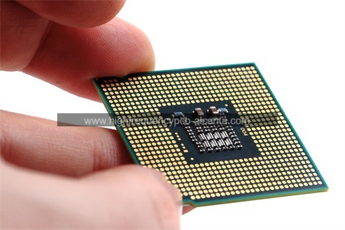
Thinnest PCB Manufacturer
Thinnest PCB Manufacturer,The thinnest PCBs are engineered to meet the demands of ultra-compact electronic devices where space is at a premium. These PCBs can achieve thicknesses as low as 0.1mm, while still maintaining mechanical integrity and electrical performance. They are crafted using advanced materials and precise manufacturing techniques to ensure reliability in high-density applications. Despite their thin profile, these PCBs offer excellent signal integrity and thermal management, making them suitable for applications such as smartphones, wearables, and medical devices. Their lightweight and slim design enable integration into sleek, space-constrained electronics without compromising functionality.
What is a Thinnest PCB?
A thinnest PCB (Printed Circuit Board) refers to a PCB that is designed to be exceptionally slim, often with a thickness less than 0.2 mm (200 microns). These ultra-thin PCBs are engineered for applications where space constraints are critical, such as in portable electronic devices, wearable technology, and compact consumer electronics.
The reduction in thickness for these PCBs involves using specialized materials and manufacturing processes. Typically, materials like flexible substrates (e.g., polyimide) or advanced composite materials are employed to achieve the desired thinness while maintaining the necessary electrical and mechanical properties. Thin PCBs can be either rigid or flexible, depending on the application requirements.
In addition to their compact size, thin PCBs must address challenges related to durability and heat dissipation. Manufacturers often use techniques like precise layer alignment, advanced etching processes, and the careful selection of dielectric materials to ensure reliability despite the reduced thickness.
The design of ultra-thin PCBs also requires careful consideration of electrical performance, as signal integrity and power distribution must be managed effectively in a constrained space. As technology continues to advance, the demand for thinner PCBs is likely to increase, pushing the boundaries of miniaturization and enabling the development of ever more compact and efficient electronic devices.
Thinnest PCB Manufacturer
What are the Thinnest PCB Design Guidelines?
Designing ultra-thin PCBs involves specific guidelines to ensure performance, reliability, and manufacturability. Here are some key considerations:
- Material Selection: Choose materials with high dielectric strength and thermal stability. Flexible substrates like polyimide or advanced composites are often used to achieve thin profiles while maintaining electrical performance.
- Layer Count:Minimize the number of layers where possible. Fewer layers reduce overall thickness and complexity. Use techniques like embedded components or thin cores to reduce layer count.
- Trace Width and Spacing: Use narrower traces and smaller spacing to fit within the thin profile constraints. Ensure that trace width and spacing adhere to manufacturing capabilities and electrical requirements to prevent issues like signal interference and overheating.
- Hole Size and Via Design: Opt for smaller via sizes or use microvias to minimize the impact on thickness. Blind and buried vias can help reduce the board’s overall thickness.
- Component Placement: Strategically place components to optimize space. Consider using smaller package sizes and low-profile components to fit within the thin PCB.
- Thermal Management: Implement effective thermal management techniques, as thinner PCBs can have limited heat dissipation. Use thermal vias, heat spreaders, or materials with high thermal conductivity to manage heat effectively.
- Mechanical Support: Thin PCBs are more prone to mechanical stress and bending. Design for mechanical stability by adding stiffeners or supports where necessary.
- Manufacturing Processes: Work closely with your PCB manufacturer to understand their capabilities and limitations for producing ultra-thin boards. Ensure that the chosen processes are compatible with the desired thickness and design requirements.
- Electrical Performance: Pay attention to signal integrity, especially with high-frequency signals. Use controlled impedance traces and consider the effects of reduced dielectric thickness on signal performance.
- Testing and Reliability:Conduct thorough testing to ensure that the thin PCB meets all reliability and performance standards. Consider factors like vibration, shock, and environmental conditions that may affect the PCB’s performance.
By following these guidelines, you can design ultra-thin PCBs that meet the needs of modern, compact electronic devices while maintaining performance and reliability.
What is the Thinnest PCB Fabrication Process?
The fabrication of the thinnest PCBs involves several specialized processes to achieve ultra-thin profiles while maintaining electrical and mechanical integrity. Here’s an overview of the typical steps involved:
- Material Selection: Start with thin, high-performance base materials. Flexible substrates like polyimide or specialized thin FR4 laminates are often chosen for their electrical properties and thinness.
- Layer Preparation: Use thin copper foils and substrates. Thin copper foils (as thin as 9 µm or 0.009 mm) are applied to the substrate to create the conductive layers. The substrate itself is prepared to be as thin as possible while maintaining structural integrity.
- Photolithography: Apply a photosensitive layer (photoresist) to the substrate. The photoresist is exposed to ultraviolet light through a mask to create the desired circuit pattern. This process is critical for defining precise trace and pad patterns.
- Etching: After exposure and development, the photoresist is used as a mask to etch away the unwanted copper. Precision etching processes, such as chemical etching or laser ablation, are employed to create fine traces and pads without damaging the thin substrate.
- Via Formation: For ultra-thin PCBs, use microvias or laser-drilled vias to minimize thickness. These vias are often formed using advanced laser drilling techniques that create very small, precise holes with minimal impact on the board’s thickness.
- Layer Alignment and Bonding: If the design requires multiple layers, align and bond them using thin bonding materials or adhesives. Techniques like thermal compression bonding or lamination under high pressure and temperature are used to ensure strong adhesion while maintaining thinness.
- Insulation and Coating: Apply thin insulation layers, such as dielectric films or conformal coatings, to protect the circuit and enhance performance. These coatings also help with electrical insulation and protection against environmental factors.
- Component Mounting: Use surface-mount technology (SMT) or other methods that accommodate thin profiles. Choose low-profile components and ensure precise placement to fit within the thin PCB constraints.
- Testing and Quality Control: Perform thorough testing, including electrical, mechanical, and thermal checks, to ensure the thin PCB meets all specifications. This includes inspecting for potential issues like signal integrity, heat dissipation, and mechanical stress.
- Finishing Processes: Apply any necessary finishing processes, such as solder mask and silkscreen layers, ensuring they are compatible with the thin profile of the PCB.
The fabrication process for the thinnest PCBs requires careful control of each step to maintain the desired thickness while ensuring performance and reliability. Advanced manufacturing techniques and close collaboration with PCB manufacturers are essential for achieving the best results.
How Do You Manufacture a Thinnest PCB?
Manufacturing the thinnest PCBs involves a series of precise and specialized steps to ensure that the boards meet the required thickness while maintaining functionality and durability. Here’s a detailed overview of the manufacturing process:
- Material Selection: Begin with selecting ultra-thin base materials, such as flexible substrates like polyimide or thin laminates of FR4 or other advanced composites. These materials should provide the necessary electrical performance and mechanical stability while being thin.
- Substrate Preparation: Cut and prepare the substrate material to the required dimensions. The substrate is often pre-coated with a thin layer of copper foil that will be used to create the circuit patterns.
- Photoresist Application: Apply a thin layer of photoresist to the copper-clad substrate. This photosensitive material will protect areas of the copper that will form the circuit patterns and allow selective etching.
- Photolithography: Expose the photoresist-coated substrate to ultraviolet light through a photomask, which defines the circuit pattern. The exposed photoresist undergoes a chemical change, allowing for selective removal in the next step.
- Development: Develop the exposed photoresist to remove the unwanted material, leaving behind the circuit pattern on the copper. This step defines the traces and pads that will form the electrical connections on the PCB.
- Etching: Use precise etching techniques, such as chemical or laser etching, to remove the exposed copper, leaving only the copper traces protected by the remaining photoresist. This step must be carefully controlled to avoid damaging the thin substrate.
- Via Formation: For multi-layer or complex designs, create vias using microvia techniques. Laser drilling is often used for its precision and ability to create very small vias with minimal impact on the board’s thickness.
- Layer Lamination: If the PCB design requires multiple layers, align and bond them using thin adhesive films or bonding materials. Lamination is performed under controlled temperature and pressure to ensure a strong bond without adding excessive thickness.
- Insulation and Coating: Apply thin dielectric materials or coatings to provide electrical insulation and protect the circuitry. Conformal coatings or thin film dielectrics can be used to cover and protect the board.
- Component Mounting: Use surface-mount technology (SMT) or other methods suited for thin PCBs. Select low-profile components and ensure they are placed with precision to fit within the thin profile constraints.
- Final Testing: Conduct comprehensive testing to ensure the thin PCB meets all performance, reliability, and quality standards. This includes electrical testing, thermal analysis, and mechanical stress testing.
- Finishing: Apply any necessary finishing touches, such as solder masks or silkscreens, ensuring they are compatible with the thin design. Final inspection and quality control are performed to confirm that the PCB meets all specifications.
Each step in the manufacturing process for the thinnest PCBs requires careful attention to detail and advanced technology to achieve the desired thinness while ensuring reliable performance and durability.
How Much Should a Thinnest PCB Cost?
The cost of manufacturing the thinnest PCBs can vary widely based on several factors:
- Thickness and Complexity: Ultra-thin PCBs, especially those with complex designs or multiple layers, generally cost more due to the specialized manufacturing processes and materials required. For instance, a PCB with a thickness of less than 0.2 mm (200 microns) will typically be more expensive than standard thickness PCBs.
- Material Costs: The choice of materials significantly impacts the cost. High-performance flexible substrates like polyimide or specialized thin laminates are more expensive than standard FR4 materials. Additionally, thin copper foils and advanced dielectric materials add to the cost.
- Layer Count and Design Complexity: Multi-layer PCBs or designs with intricate circuit patterns require advanced manufacturing techniques, which increase costs. Microvias and precision etching also contribute to higher production costs.
- Manufacturing Processes: Advanced processes such as laser drilling for microvias, fine-line etching, and precise photolithography are more expensive than standard PCB processes. The need for specialized equipment and expertise raises the overall cost.
- Quantity: The cost per unit typically decreases with higher production volumes. Small batch or prototype runs for ultra-thin PCBs can be significantly more expensive on a per-unit basis compared to larger production runs.
- Testing and Quality Assurance: Comprehensive testing and quality control measures are crucial for thin PCBs to ensure reliability and performance. These additional steps add to the cost of manufacturing.
To get a precise cost estimate, it’s best to consult with PCB manufacturers who specialize in ultra-thin designs. They can provide detailed quotes based on your specific design requirements, materials, and production volume.
What is Thinnest PCB Base Material?
The thinnest PCB base materials are designed to provide electrical performance and mechanical stability while maintaining an ultra-thin profile. Here are some commonly used materials for manufacturing the thinnest PCBs:
- Polyimide: This is a flexible substrate material known for its excellent thermal stability and electrical insulation properties. Polyimide can be manufactured to very thin thicknesses, often as low as 0.05 mm (50 microns), making it ideal for ultra-thin flexible PCBs.
- FR4 Laminates:While traditional FR4 is thicker, specialized thin FR4 laminates can be used for applications requiring rigid boards with minimal thickness. These can be produced in thicknesses down to around 0.1 mm (100 microns).
- Rogers Materials: Rogers Corporation offers high-frequency laminate materials like Rogers 4003C and 4350B, which are known for their excellent electrical properties. These can be available in thinner versions suitable for high-performance thin PCBs, although typically used for specific applications.
- Flexible PCB Materials: Materials such as PET (Polyethylene Terephthalate) or PI (Polyimide) films are used for ultra-thin and flexible PCBs. These films can be as thin as 25 microns (0.025 mm) and are used in applications where flexibility and ultra-thin profiles are critical.
- High-TG Epoxy Materials: For applications requiring higher thermal performance, high-TG (glass transition temperature) epoxy materials can be used. These materials can be manufactured in thinner configurations to support high thermal performance in thin PCB designs.
- Ceramic Substrates: Thin ceramic substrates, such as aluminum nitride (AlN) or beryllium oxide (BeO), are used for high-performance applications where heat dissipation is crucial. These materials can be quite thin, though typically more rigid and used in specific high-frequency or high-power applications.
When selecting a base material for ultra-thin PCBs, it’s important to consider not only the thickness but also the material’s electrical properties, thermal performance, and mechanical characteristics to ensure it meets the specific needs of your application.
Which Company Makes Thinnest PCBs?
Here are some well-known companies that manufacture ultra-thin PCBs:
- Axiom Electronics: Specializes in producing various types of PCBs, including ultra-thin ones. Their products are widely used in consumer electronics, medical devices, and industrial applications.
- Flex Ltd.: A global leader in electronic manufacturing services, providing various PCB solutions including ultra-thin flexible PCBs. Their thin PCBs are widely used in smartphones, wearables, and other devices.
- Zhen Ding Technology Holding Limited: A company with strong technical capabilities in PCB manufacturing, capable of producing ultra-thin PCBs, particularly excelling in high-frequency and high-performance areas.
- AT&S: An international leading PCB manufacturer offering various products including ultra-thin PCBs. Their ultra-thin PCBs have widespread applications in high-tech and medical fields.
- Nippon Mektron: A globally recognized flexible PCB manufacturer that provides various ultra-thin PCB solutions, widely used in electronic consumer goods and industrial equipment.
- Unimicron Technology Corp.: This company has extensive experience in manufacturing ultra-thin PCBs and offers solutions suitable for high-frequency and high-density applications.
Our company specializes in manufacturing ultra-thin PCBs. With advanced production processes and material technologies, we are capable of producing PCBs with thicknesses as low as 0.1 mm (100 microns). Our manufacturing capabilities cover a range of types from flexible to rigid PCBs, meeting the needs of various industries and applications.
We utilize high-precision photolithography and chemical etching processes to ensure the electrical performance and mechanical stability of ultra-thin PCBs. For material selection, we use high-performance polyimide (PI) films and customized thin FR4 substrates to maintain excellent electrical performance and durability even at minimal thicknesses.
Additionally, our production process includes rigorous quality control and testing procedures to ensure that each ultra-thin PCB meets high standards of reliability and performance. Whether for consumer electronics, medical devices, or industrial applications, we provide tailored solutions to meet the specific needs of our clients.
What Are the 7 Qualities of Good Customer Service?
Good customer service is crucial for building strong relationships with customers and ensuring their satisfaction. Here are seven key qualities of excellent customer service:
- Responsiveness: Promptly addressing customer inquiries, concerns, and issues is essential. Quick responses show that you value the customer’s time and are committed to resolving their problems efficiently.
- Empathy: Understanding and relating to the customer’s feelings and experiences is crucial. Empathy involves listening actively and showing genuine concern for their issues, which helps build trust and rapport.
- Communication Skills: Clear, concise, and effective communication is vital. This includes being able to explain information in an understandable way, listening attentively, and using positive language to create a friendly and professional interaction.
- Knowledge: Providing accurate and helpful information requires in-depth knowledge of products, services, and company policies. Staff should be well-trained to offer insightful answers and solutions to customer inquiries.
- Patience: Handling customer interactions with patience, especially when dealing with difficult or frustrated customers, is essential. Remaining calm and composed helps in addressing issues more effectively and maintaining a positive relationship.
- Reliability:Consistently delivering on promises and commitments builds trust. Customers should be able to rely on the company to follow through on its promises, whether it’s meeting deadlines, honoring warranties, or providing accurate information.
- Personalization: Tailoring interactions to meet the individual needs and preferences of customers enhances their experience. Personalization involves remembering previous interactions, addressing customers by name, and offering solutions that are relevant to their specific situation.
By incorporating these qualities, companies can create a positive customer experience that fosters loyalty and satisfaction.
FAQs
What is a Thinnest PCB?
A Thinnest PCB is a printed circuit board designed to be as thin as possible while maintaining its functionality.
How do I choose the right Thinnest PCB material?
Consider the application requirements, including flexibility, thermal management, and electrical performance.
Can Thinnest PCBs be used in high-frequency applications?
Yes, but ensure the material and design are optimized for high-frequency performance.
What factors affect the cost of a Thinnest PCB?
Design complexity, material quality, order quantity, and manufacturing processes all influence the cost.
How can I ensure the quality of my Thinnest PCB?
Work with reputable manufacturers and conduct thorough testing during and after production.