 Professional high frequency circuit board supplier
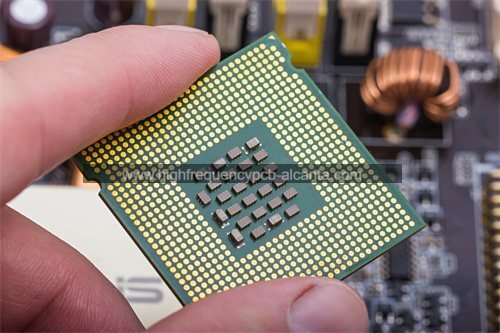
What is SOP Package Substrate?
SOP Package Substrate Manufacturer,SOP (Small Outline Package) substrate is a compact solution for semiconductor packaging, optimizing space and performance. Featuring precise dimensions, it enables high-density mounting on circuit boards, reducing overall system footprint. SOP substrates ensure reliable electrical connections and mechanical stability, critical for compact electronic devices like smartphones and tablets. With efficient heat dissipation, they support high-speed operation and enhance system performance. SOP package substrates are widely used in consumer electronics, IoT, and automotive applications, where space-saving and reliability are paramount. Their compact design and advanced materials facilitate the development of smaller, lighter, and more efficient electronic products for diverse applications.
SOP (Small Outline Package) is a type of integrated circuit (IC) package used in semiconductor manufacturing. The SOP package substrate refers to the material layer or structure on which the integrated circuit chip is mounted within the SOP package.
The substrate serves several functions:
Mechanical Support: It provides a solid foundation for mounting the IC chip and other package components.
Electrical Connections: The substrate typically contains conductive traces (often made of copper) that connect the IC chip to the package’s external pins or leads. These traces facilitate the flow of electrical signals between the chip and the external environment.
Heat Dissipation: The substrate may also play a role in dissipating heat generated by the IC chip during operation. This is particularly important in high-performance applications where excessive heat can degrade the performance or reliability of the device.
Overall, the SOP package substrate is an essential component in the packaging of integrated circuits, providing mechanical support, electrical connectivity, and thermal management for the chip.
SOP Package Substrate Manufacturer
What are the Functions of SOP Package Substrate?
The SOP (Small Outline Package) package substrate serves several important functions in the packaging of integrated circuits:
Mechanical Support: The substrate provides a sturdy platform for mounting the integrated circuit (IC) chip and other package components. It ensures that the chip remains securely in place within the package, even during handling and operation.
Electrical Connectivity: The substrate contains conductive traces or wiring that connect the various terminals of the IC chip to the package’s external pins or leads. These connections enable the transfer of electrical signals between the IC chip and the external circuitry, allowing the device to function as intended.
Signal Routing: The substrate routes electrical signals between different parts of the IC chip and the external pins or leads of the package. This routing ensures that signals are directed to the appropriate locations within the package and the external circuitry, facilitating proper communication and operation of the device.
Thermal Management: In many cases, the substrate plays a role in dissipating heat generated by the IC chip during operation. It may include features such as thermal vias, thermal pads, or heat spreaders that help conduct heat away from the chip and distribute it more evenly throughout the package. Effective thermal management is crucial for maintaining the reliability and performance of the device, particularly in high-power or high-speed applications.
Environmental Protection: The substrate may also provide a degree of protection for the IC chip against environmental factors such as moisture, dust, and mechanical shocks. It helps shield the sensitive semiconductor components from external damage, thereby improving the overall durability and longevity of the device.
Overall, the SOP package substrate plays a critical role in ensuring the functionality, reliability, and longevity of integrated circuit packages by providing mechanical support, electrical connectivity, signal routing, thermal management, and environmental protection for the IC chip.
What are the Different Types of SOP Package Substrate?
There are several types of SOP (Small Outline Package) package substrates, each designed for specific applications and requirements. Some common types include:
SOP: The standard SOP package typically features a rectangular or square shape with leads extending from two opposite sides.
SSOP (Shrink Small Outline Package): SSOP packages have smaller lead pitches and overall dimensions compared to standard SOP packages, making them suitable for applications where space is limited.
TSOP (Thin Small Outline Package): TSOP packages are characterized by their thin profile, making them suitable for applications where height constraints are important, such as in portable electronic devices.
TSSOP (Thin Shrink Small Outline Package): TSSOP packages combine the thin profile of TSOP packages with the smaller lead pitches of SSOP packages, offering a compact form factor suitable for space-constrained applications.
MSOP (Mini Small Outline Package): MSOP packages are even smaller than SSOP packages, making them ideal for compact designs or applications where board space is limited.
HSOP (Heat Sink Small Outline Package): HSOP packages feature additional thermal management features, such as heat sinks or exposed pads, to improve heat dissipation and thermal performance.
These are just a few examples of the various SOP package substrates available, each tailored to specific requirements such as size, pitch, and thermal performance. The choice of substrate depends on factors such as the application’s space constraints, electrical requirements, and thermal management needs.
How does SOP Package Substrate Relate to IC Packaging?
The SOP (Small Outline Package) package substrate is an integral part of IC (Integrated Circuit) packaging. IC packaging involves encapsulating and protecting the semiconductor chip (IC) and providing electrical connections to external circuitry. The package substrate plays several crucial roles in this process:
Mechanical Support: The substrate provides a sturdy foundation for mounting the IC chip and other package components, such as wire bonds or solder balls. It ensures that the chip remains securely in place within the package, protecting it from physical damage.
Electrical Connections: The substrate typically contains conductive traces that connect the IC chip to the package’s external leads or pins. These traces serve as pathways for electrical signals to flow between the chip and the external environment, allowing the IC to communicate with other components or devices.
Thermal Management: In many cases, the substrate also assists in dissipating heat generated by the IC chip during operation. Heat can degrade the performance and reliability of semiconductor devices, so effective thermal management is essential. Some substrates may incorporate features such as heat sinks, thermal vias, or exposed pads to enhance heat dissipation.
Signal Integrity: The design of the substrate, including the layout of the conductive traces and the arrangement of components, can impact signal integrity. Proper design techniques are employed to minimize signal distortion, crosstalk, and other electrical issues that may affect the performance of the IC.
Overall, the SOP package substrate plays a critical role in IC packaging by providing mechanical support, facilitating electrical connections, managing thermal properties, and ensuring signal integrity. Its design and construction are carefully optimized to meet the specific requirements of the IC and its intended application.
What are the Differences Between SOP Package Substrate and PCB?
SOP (Small Outline Package) package substrate and PCB (Printed Circuit Board) are both essential components in electronic devices, but they serve different functions and have distinct characteristics. Here are the key differences between them:
Function:
SOP Package Substrate: The SOP package substrate primarily serves as a mounting platform and electrical connection interface for integrated circuit (IC) chips within semiconductor packages. It provides mechanical support, electrical connections, and thermal management for the IC.
PCB: A PCB is a board made of insulating material (such as fiberglass or epoxy) with conductive traces printed or etched onto its surface. PCBs serve as the backbone of electronic circuits, providing a platform for mounting various components (including ICs), routing electrical connections between them, and providing mechanical support.
Size and Shape:
SOP Package Substrate: SOP package substrates are typically small and compact, designed to fit within the dimensions of the semiconductor package they are used in. They often have a rectangular or square shape.
PCB: PCBs come in various sizes and shapes, depending on the specific application and requirements. They can range from small boards used in consumer electronics to large boards used in industrial or telecommunications equipment.
Integration:
SOP Package Substrate: The substrate is integrated directly into the semiconductor package during the manufacturing process. It is closely coupled with the IC chip and other package components.
PCB: PCBs are separate components that can be populated with various electronic components, including ICs, resistors, capacitors, and connectors. They are often designed to accommodate multiple components and complex circuitry.
Complexity and Layering:
SOP Package Substrate: SOP package substrates are typically simpler in design and construction compared to PCBs. They may consist of a single layer or multiple layers, depending on the requirements of the semiconductor package.
PCB: PCBs can be highly complex, with multiple layers of conductive traces and insulating material (known as copper layers and dielectric layers, respectively). Multilayer PCBs allow for dense routing of electrical connections and support more sophisticated circuit designs.
In summary, while both SOP package substrates and PCBs play crucial roles in electronic devices, they serve different functions and have distinct characteristics in terms of size, integration, complexity, and construction.
What are the Main Structures and Production Technologies of SOP Package Substrate?
The main structures and production technologies of SOP (Small Outline Package) package substrates can vary depending on the specific requirements of the semiconductor package and the integrated circuit (IC) it houses. However, there are some common structures and production technologies used in the manufacture of SOP package substrates:
Basic Structure:
Substrate Material: SOP package substrates are typically made of a material with good thermal conductivity and electrical insulation properties, such as FR-4 (fiberglass-reinforced epoxy), ceramics, or laminate materials.
Conductor Traces: Conductive traces made of materials like copper are patterned on the substrate to provide electrical connections between the IC chip and the external leads or pins of the package.
Dielectric Layers: Insulating layers separate the conductor traces to prevent short circuits and provide mechanical support.
Production Technologies:
Laser Drilling: Laser drilling is used to create small holes in the substrate for via formation, allowing for the connection of conductive traces between different layers of the substrate.
Copper Deposition and Etching: Copper is deposited onto the substrate surface using techniques such as electroplating or sputtering. The excess copper is then etched away to form the desired conductor trace patterns.
Photoresist Patterning: Photoresist is applied to the substrate surface and exposed to UV light through a mask, defining the areas where copper will be deposited or removed during the etching process.
Via Formation: Vias are created by drilling small holes through the substrate and filling them with conductive material to establish electrical connections between different layers of the substrate.
Surface Finish: The substrate surface is treated with a surface finish to protect the copper traces from oxidation and improve solderability. Common surface finishes include HASL (Hot Air Solder Leveling), ENIG (Electroless Nickel Immersion Gold), and OSP (Organic Solderability Preservatives).
Additional Features:
Thermal Management Structures: Depending on the thermal requirements of the IC package, additional features such as heat sinks, thermal vias, or exposed pads may be incorporated into the substrate design to enhance heat dissipation.
Fine Pitch Traces: Advanced production technologies enable the fabrication of SOP package substrates with fine pitch traces, allowing for higher-density packaging of ICs.
Overall, SOP package substrates are manufactured using a combination of precision fabrication techniques, including laser drilling, copper deposition and etching, photoresist patterning, via formation, and surface finishing, to meet the specific requirements of the semiconductor package and ensure reliable electrical performance.
Frequently Asked Questions (FAQs)
What is an SOP package substrate?
An SOP package substrate is a component within semiconductor packaging that provides mechanical support, electrical connections, and thermal management for integrated circuit (IC) chips. It serves as a mounting platform for the IC within the semiconductor package.
What are the main functions of an SOP package substrate?
The main functions of an SOP package substrate include providing mechanical support to the IC chip, facilitating electrical connections between the chip and the package’s external leads or pins, and managing heat generated by the chip during operation.
What are the different types of SOP package substrates?
SOP package substrates come in various types, including standard SOP, SSOP (Shrink Small Outline Package), TSOP (Thin Small Outline Package), TSSOP (Thin Shrink Small Outline Package), MSOP (Mini Small Outline Package), and HSOP (Heat Sink Small Outline Package). Each type has specific characteristics suited for different applications and requirements.
What are the differences between SOP package substrates and PCBs?
SOP package substrates are components integrated directly into semiconductor packages, providing support and connectivity for IC chips. PCBs (Printed Circuit Boards), on the other hand, are separate boards that serve as the foundation for electronic circuits, accommodating various components and facilitating interconnections between them.
What are the main structures and production technologies of SOP package substrates?
SOP package substrates typically consist of insulating material (such as epoxy resin) with conductive traces (often made of copper) patterned on the surface. Production technologies may include processes like etching, plating, and dielectric layer deposition to create the necessary structures and connections on the substrate.
Conclusion
In conclusion, SOP (Small Outline Package) package substrates play a crucial role in semiconductor packaging, providing mechanical support, electrical connectivity, and thermal management for integrated circuit (IC) chips. They come in various types and are essential components in electronic devices, facilitating the integration and functionality of ICs within semiconductor packages. Understanding the functions, types, differences from PCBs, and production technologies of SOP package substrates is essential for those involved in semiconductor manufacturing and electronic design.