 Professional high frequency circuit board supplier
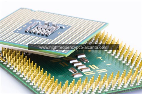
What is SIP Package Substrate?
SIP Package Substrate Manufacturer,SIP (System-in-Package) substrate integrates multiple semiconductor components into a single module, optimizing space and performance. These substrates offer compact designs, enabling high-density mounting and reducing interconnect length. SIP substrates ensure efficient heat dissipation, reliable electrical connections, and mechanical stability. Widely used in mobile devices, IoT, and wearable technology, SIP package substrates support miniaturization and enhance system functionality. Their advanced construction and precise assembly enable seamless integration of diverse components, ensuring superior performance and reliability in modern electronic devices. SIP substrates drive advancements in electronic packaging, enabling the development of smaller, lighter, and more efficient products for various applications.
SIP (System in Package) package substrate is the physical foundation or base upon which the various components of an integrated circuit (IC) are mounted and connected. It serves as a platform for assembling multiple chips, including microprocessors, memory modules, and other integrated circuits, into a single package. The substrate provides electrical connections between the chips and facilitates the transmission of signals and power between them.
SIP package substrates are typically made of materials such as organic laminate, ceramic, or silicon, depending on the specific requirements of the application. They may also include additional features such as through-silicon vias (TSVs) for vertical interconnections between stacked chips, thermal management structures, and routing layers for signal distribution.
Overall, SIP package substrates play a critical role in enabling the integration of multiple chips into compact and efficient packages, which can help reduce the overall size, cost, and power consumption of electronic devices.
SIP Package Substrate Manufacturer
What are the functions of SIP Package Substrate?
The SIP package substrate serves several important functions in the overall functionality and performance of the integrated components within the package:
Electrical Interconnection: The substrate provides the electrical connections between the various components integrated into the SIP package. These connections enable data transfer, power distribution, and communication between different parts of the package.
Thermal Management: Efficient thermal management is crucial for the reliable operation of electronic components. The substrate helps in dissipating heat generated by the components, ensuring they operate within their specified temperature range and preventing overheating that could degrade performance or lead to failure.
Mechanical Support: The substrate provides mechanical support for the components mounted on it, ensuring they are securely held in place within the package. This support helps prevent damage to the components due to mechanical stress or vibration during operation or handling.
Signal Integrity: Maintaining signal integrity is essential for the reliable transmission of data and communication between components within the SIP package. The substrate plays a role in minimizing signal distortion and interference, ensuring that signals remain accurate and stable.
Power Distribution: The substrate facilitates the distribution of power to the various components within the SIP package, ensuring they receive the required voltage and current for proper operation.
Integration and Miniaturization: By integrating multiple components into a single package and providing a platform for their interconnection, the substrate enables the miniaturization of electronic devices. This allows for the development of smaller and more compact products without compromising functionality or performance.
Overall, the SIP package substrate plays a crucial role in enabling the integration, functionality, and reliability of electronic components within a single package, contributing to the performance and efficiency of electronic devices.
What are the different types of SIP Package Substrate?
There are several different types of substrates used in SIP (System in Package) packages, each with its own characteristics and suitability for specific applications. Some common types of SIP package substrates include:
Organic Substrates: Organic substrates are typically made of materials such as FR-4 (Flame Retardant-4), epoxy resins, or polyimide. These substrates are cost-effective, lightweight, and offer good electrical insulation properties. Organic substrates are commonly used in consumer electronics and low- to mid-range applications.
Ceramic Substrates: Ceramic substrates, such as alumina (Al2O3) or aluminum nitride (AlN), offer excellent thermal conductivity and mechanical strength. They are highly stable across a wide temperature range and provide superior thermal management capabilities. Ceramic substrates are often used in high-performance applications such as automotive electronics, aerospace, and high-power electronic devices.
Flexible Substrates: Flexible substrates, such as polyimide or polyester films, offer flexibility and conformability, making them suitable for applications where space constraints or curved surfaces are present. Flexible substrates are commonly used in wearable devices, medical electronics, and other applications requiring bendable or stretchable electronics.
Copper Substrates: Copper substrates, also known as copper core substrates or copper-clad laminates, feature a layer of copper bonded to an insulating substrate material. These substrates offer excellent thermal conductivity and are often used in high-power applications such as power amplifiers, RF modules, and LED lighting.
Metal Core Substrates (MCPCB): Metal core substrates typically consist of a layer of metal, such as aluminum or copper, sandwiched between layers of insulating material. These substrates provide efficient heat dissipation and mechanical stability, making them suitable for high-power LED lighting, automotive lighting, and power electronics applications.
Glass Substrates: Glass substrates offer high dimensional stability, excellent electrical insulation properties, and compatibility with high-temperature processing. They are commonly used in applications requiring high reliability, such as automotive electronics, aerospace, and medical devices.
The choice of substrate type depends on factors such as thermal management requirements, electrical performance, mechanical constraints, and cost considerations, among others. Each type of substrate offers different advantages and is selected based on the specific needs of the application.
What is the relationship between SIP Package Substrate and IC packaging?
SIP (System in Package) package substrate and IC (Integrated Circuit) packaging are closely related as they both involve the integration and packaging of multiple electronic components into a single module. However, there are some differences in their scope and focus:
SIP Package Substrate: The substrate in an SIP package serves as the foundation or platform on which the integrated components are mounted and interconnected. It provides electrical connections, thermal management, mechanical support, and signal integrity for the components within the package. The substrate in an SIP package plays a crucial role in enabling the integration, functionality, and reliability of electronic components within a single package.
IC Packaging: IC packaging encompasses the entire process of enclosing and protecting individual integrated circuits (ICs) or chips. This includes various steps such as die attachment, wire bonding or flip-chip bonding, encapsulation with molding compounds, and lead frame or ball grid array (BGA) formation. IC packaging ensures the reliability, electrical connectivity, thermal performance, and mechanical protection of the ICs.
The relationship between SIP package substrate and IC packaging lies in the fact that the substrate is an essential component within the overall IC packaging process, particularly in the case of SIP packages. The substrate provides the platform for mounting and interconnecting multiple ICs or components within the package, thereby contributing to the functionality, performance, and reliability of the packaged device.
In summary, while IC packaging refers to the broader process of enclosing individual ICs, SIP package substrate specifically refers to the material or platform used for integrating and interconnecting multiple components within a single package, playing a crucial role in the overall IC packaging process.
How does SIP Package Substrate differ from PCB?
SIP Package Substrate and PCB (Printed Circuit Board) are both foundational elements in electronics assembly, but they serve different purposes and have distinct characteristics:
Functionality:
SIP Package Substrate: The substrate in a SIP package serves as the foundation on which multiple electronic components are integrated into a single package. It facilitates electrical connections, thermal management, mechanical support, and signal integrity within the package.
PCB: A PCB, on the other hand, is a standalone board that provides electrical connections between various electronic components. It serves as the platform for mounting and interconnecting components such as integrated circuits (ICs), resistors, capacitors, and other electronic devices. PCBs can have multiple layers, with copper traces etched onto the surface to create electrical pathways.
Integration:
SIP Package Substrate: SIP packages integrate multiple components, such as ICs, passive components, and sometimes even MEMS (Micro-Electro-Mechanical Systems) devices, into a single package. The substrate plays a crucial role in enabling this integration by providing a platform for mounting and interconnecting these components.
PCB: PCBs typically integrate various discrete electronic components onto a single board, but they do not encapsulate these components into a single package. PCBs are commonly used in electronic devices such as computers, smartphones, and industrial equipment to provide the necessary electrical connections and support for the components.
Material and Design:
SIP Package Substrate: SIP package substrates are often made of materials such as organic substrates (e.g., FR-4), ceramics (e.g., alumina), or metal-core substrates. The choice of substrate material depends on factors such as thermal management requirements, signal integrity, and cost considerations.
PCB: PCBs are typically made of layers of fiberglass or other dielectric materials with copper traces patterned onto the surface. They can have multiple layers interconnected through vias to facilitate complex electronic circuits. PCBs can also incorporate various technologies such as through-hole mounting or surface-mount technology (SMT) for component attachment.
Application:
SIP Package Substrate: SIP packages are often used in applications where space, weight, and performance are critical factors, such as mobile devices, wearables, automotive electronics, and IoT (Internet of Things) devices.
PCB: PCBs are used in a wide range of electronic devices and systems across various industries, including consumer electronics, telecommunications, aerospace, automotive, medical devices, and industrial equipment.
In summary, while both SIP package substrate and PCB are essential elements in electronics assembly, they serve different purposes and are used in different applications. SIP package substrate focuses on integrating multiple components into a single package, while PCB provides the platform for mounting and interconnecting components in electronic circuits.
What are the structure and production technology of SIP Package Substrate?
The structure and production technology of SIP (System in Package) package substrates can vary depending on the specific requirements of the application and the type of substrate being used. However, here is a general overview of the structure and production technology:
Structure:
Base Material: The base material of SIP package substrates can vary and may include organic substrates (e.g., FR-4), ceramics (e.g., alumina or aluminum nitride), metal-core substrates, or flexible substrates (e.g., polyimide).
Dielectric Layers: Depending on the substrate type, one or more dielectric layers may be added on top of the base material. These layers provide insulation and mechanical support for the conductive traces and components mounted on the substrate.
Conductive Traces: Conductive traces, typically made of copper, are patterned onto the substrate to provide electrical connections between the integrated components within the SIP package. These traces may be formed using techniques such as etching or additive processes.
Mounting Pads: Mounting pads or landing pads are areas on the substrate where the integrated components are attached or soldered. These pads provide mechanical support and electrical connectivity for the components.
Through-Hole Vias or Microvias: Depending on the substrate’s design and complexity, through-hole vias or microvias may be incorporated to facilitate vertical electrical connections between different layers of the substrate.
Surface Finish: The surface of the substrate may be coated with a surface finish to protect the conductive traces from oxidation and facilitate soldering of components during assembly.
Production Technology:
Substrate Fabrication: The production of SIP package substrates typically begins with the fabrication of the base material, which may involve processes such as lamination, pressing, or deposition of materials onto a substrate surface.
Laser Drilling or Mechanical Drilling: Holes or vias may be drilled into the substrate using laser drilling or mechanical drilling techniques to create pathways for electrical connections between different layers.
Copper Deposition and Etching: Conductive traces are formed on the substrate by depositing a layer of copper onto the surface through techniques such as electroplating or sputtering. The copper is then patterned using photolithography and etching processes to create the desired circuitry.
Surface Finish Application: After the circuitry is formed, a surface finish may be applied to the substrate to protect the copper traces and facilitate component soldering. Common surface finishes include HASL (Hot Air Solder Leveling), ENIG (Electroless Nickel Immersion Gold), and OSP (Organic Solderability Preservatives).
Component Attachment: Once the substrate is prepared, electronic components such as integrated circuits (ICs), passive components, and MEMS devices are mounted onto the substrate using techniques such as wire bonding, flip-chip bonding, or soldering.
Encapsulation: In some cases, the assembled components may be encapsulated with a molding compound to protect them from environmental factors such as moisture, dust, and mechanical stress.
Overall, the production technology of SIP package substrates involves a combination of material processing, patterning, and assembly techniques to create a platform for integrating multiple electronic components into a single package. The specific processes and materials used may vary depending on the substrate type and the requirements of the application.
Frequently Asked Questions (FAQs)
What is SIP Package Substrate?
SIP Package Substrate refers to the material or platform used for integrating multiple electronic components into a single package. It provides electrical connections, thermal management, mechanical support, and signal integrity for the components within the package.
What are the functions of SIP Package Substrate?
The functions of SIP Package Substrate include electrical interconnection, thermal management, mechanical support, signal integrity maintenance, power distribution, and integration for miniaturization.
What are the different types of SIP Package Substrate?
Common types of SIP Package Substrate include organic substrates, ceramic substrates, flexible substrates, copper substrates, metal core substrates (MCPCB), and glass substrates.
How does SIP Package Substrate differ from PCB?
SIP Package Substrate focuses on integrating multiple components into a single package, providing functionality and reliability within a compact form factor. PCB, on the other hand, is a standalone board that provides electrical connections between various electronic components in a circuit.
What is the relationship between SIP Package Substrate and IC packaging?
SIP Package Substrate is an essential component within the overall IC packaging process. It provides the platform for mounting and interconnecting multiple integrated circuits (ICs) or components within a single package, contributing to functionality, performance, and reliability.
What is the structure and production technology of SIP Package Substrate?
The structure of SIP Package Substrate typically includes base material, dielectric layers, conductive traces, mounting pads, through-hole vias or microvias, and surface finish. Production technology involves substrate fabrication, drilling, copper deposition and etching, surface finish application, component attachment, and encapsulation.
Conclusion
In conclusion, SIP (System in Package) Package Substrate is a critical component in electronics assembly, enabling the integration of multiple electronic components into a single package. It provides essential functions such as electrical interconnection, thermal management, mechanical support, signal integrity maintenance, and power distribution. SIP Package Substrate comes in various types, including organic substrates, ceramic substrates, flexible substrates, copper substrates, metal core substrates, and glass substrates, each with its own characteristics and suitability for different applications.
While SIP Package Substrate shares similarities with PCB (Printed Circuit Board) in terms of providing electrical connections and support for electronic components, it differs in focus and scope. SIP Package Substrate specifically focuses on integrating multiple components into a single package, while PCB serves as a standalone board for mounting and interconnecting components in electronic circuits.
The relationship between SIP Package Substrate and IC packaging is significant, as the substrate plays a crucial role within the overall IC packaging process, providing the platform for mounting and interconnecting multiple integrated circuits or components within a single package.
The structure of SIP Package Substrate typically includes base material, dielectric layers, conductive traces, mounting pads, through-hole vias or microvias, and surface finish. Production technology involves substrate fabrication, drilling, copper deposition and etching, surface finish application, component attachment, and encapsulation.
Overall, SIP Package Substrate plays a vital role in enabling the integration, functionality, and reliability of electronic components within a single package, contributing to the performance and efficiency of electronic devices across various industries.