 Professional high frequency circuit board supplier
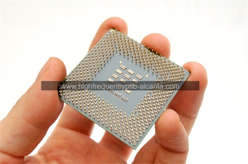
What is Semiconductor Package Substrate?
Semiconductor Package Substrate Manufacturer,Semiconductor package substrates are essential components in microelectronics, providing the foundational platform for mounting and interconnecting semiconductor chips. These substrates are designed with multiple layers of conductive traces and insulating materials, ensuring reliable electrical performance and signal integrity. They offer excellent thermal dissipation, mechanical support, and protection for delicate semiconductor devices. Commonly made from materials like BT resin, ceramics, or organic substrates, semiconductor package substrates cater to various applications, including computing, telecommunications, and automotive electronics. They enable miniaturization and high-density integration, ensuring durability and efficiency in modern electronic systems.
A semiconductor package substrate is a crucial component in semiconductor packaging, serving as the foundation for mounting and interconnecting various semiconductor devices within a package. It acts as a platform for connecting the integrated circuit (IC) or chip to the rest of the package, as well as to the external circuitry.
The substrate provides electrical connections between the chip and the package’s leads or pins, as well as thermal management functions to dissipate heat generated by the chip during operation. It typically consists of a thin, flat material, such as a ceramic or laminate material, with layers of conductive traces (usually made of copper) patterned on its surface. These traces form the interconnections between the chip and the package’s external pins or leads.
Semiconductor package substrates come in various forms, including:
Printed Circuit Board (PCB): PCB substrates are made of insulating material (such as fiberglass epoxy) with copper traces patterned on the surface. PCB substrates are commonly used in packaging for high pin count and high-performance applications.
Ceramic Substrates: Ceramic substrates offer excellent thermal performance and mechanical stability, making them suitable for high-power and high-frequency applications. They are often used in applications where thermal dissipation is critical.
Lead Frame: Lead frames are metal frames with leads or pins protruding from the edges. They provide mechanical support and electrical connections for the chip. Lead frames are commonly used in packages such as Dual in-line Packages (DIPs) and Quad Flat Packages (QFPs).
Organic Substrates: Organic substrates, such as laminate materials like FR-4, offer cost-effective solutions for semiconductor packaging. They are widely used in consumer electronics and other applications where cost is a significant factor.
The choice of substrate depends on various factors including performance requirements, cost considerations, and application-specific needs. As semiconductor technology advances, the development of advanced substrate materials and packaging techniques continues to play a vital role in enabling higher performance, smaller form factors, and increased functionality in semiconductor devices.
Semiconductor Package Substrate Manufacturer
What are the functions of Semiconductor Package Substrate?
A semiconductor package substrate, often referred to simply as a substrate, is a key component in semiconductor packaging technology. It serves several important functions:
Electrical Connection: One of the primary functions of the substrate is to provide electrical connections between the semiconductor die (the integrated circuit) and the rest of the system. These connections are typically made through wire bonding, flip-chip bonding, or other interconnection techniques.
Heat Dissipation: Semiconductor devices generate heat during operation, and efficient heat dissipation is crucial for maintaining optimal performance and reliability. The substrate can serve as a heat sink, helping to dissipate heat away from the semiconductor die to the surrounding environment.
Mechanical Support: The substrate provides mechanical support for the semiconductor die, protecting it from physical damage and ensuring proper alignment within the package.
Signal Routing: In more complex semiconductor packages, such as multi-chip modules (MCMs) or system-in-package (SiP) configurations, the substrate facilitates the routing of signals between different components within the package. This includes providing paths for power distribution, clock signals, and data communication.
Integration of Passive Components: Substrates often incorporate passive components such as resistors, capacitors, and inductors to support the functionality of the semiconductor device. These components may be integrated directly into the substrate to save space and improve electrical performance.
Electrical Isolation and Signal Integrity: The substrate plays a role in isolating different electrical signals from each other to prevent interference and maintain signal integrity. It may include layers of insulation or shielding to minimize cross-talk and electromagnetic interference (EMI).
Overall, the semiconductor package substrate is a critical component that enables the integration, protection, and efficient operation of semiconductor devices in various electronic systems. Its design and materials are carefully chosen to meet the specific requirements of the application, balancing factors such as electrical performance, thermal management, and mechanical robustness.
What are the different types of Semiconductor Package Substrate?
Semiconductor package substrates come in various types, each tailored to specific applications and packaging technologies. Here are some common types:
Printed Circuit Board (PCB):
Single-Layer PCB: Consists of a single layer of substrate material, typically fiberglass (FR4) or other rigid materials. Used in simpler semiconductor packages.
Multi-Layer PCB: Contains multiple layers of substrate material with conductive traces sandwiched between them. Provides increased routing density and improved signal integrity. Commonly used in complex semiconductor packages like ball grid arrays (BGAs) and chip-scale packages (CSPs).
Ceramic Substrates:
Alumina (Al2O3): A popular ceramic material known for its excellent thermal conductivity and mechanical strength. Alumina substrates are commonly used in high-power semiconductor packages.
Aluminum Nitride (AlN): Offers even better thermal conductivity than alumina and is suitable for applications requiring superior heat dissipation, such as high-frequency and high-power devices.
LTCC (Low-Temperature Co-fired Ceramic): A type of ceramic substrate fabricated using a co-firing process at relatively low temperatures. LTCC substrates are used in applications requiring integration of passive components and high-frequency performance.
Organic Substrates:
BGA Substrate: Ball grid array substrates typically consist of an organic substrate material with a grid of solder balls attached to the bottom for surface mount assembly.
FCBGA (Flip Chip Ball Grid Array) Substrate: Similar to BGA substrates but designed specifically for flip-chip packaging, where the semiconductor die is flipped and attached directly to the substrate.
FC-CSP (Flip Chip Chip-Scale Package) Substrate: A variant of flip-chip packaging where the substrate size closely matches the size of the semiconductor die, resulting in a compact package with minimal footprint.
Metal Substrates:
Metal Core PCB (MCPCB): Consists of a metal core, typically aluminum or copper, sandwiched between layers of insulating material. MCPCBs are used in applications requiring efficient heat dissipation, such as high-power LEDs and power electronic devices.
Flexible Substrates:
Flexible PCB (Flex PCB): Made of flexible substrate materials like polyimide (PI) or polyester (PET). Flex PCBs are used in applications where bending or conforming to non-planar surfaces is necessary, such as wearable electronics and flexible displays.
These are some of the main types of semiconductor package substrates, each offering different characteristics suited to specific requirements such as thermal management, electrical performance, and form factor constraints. The choice of substrate type depends on factors such as the application, performance requirements, cost considerations, and manufacturing capabilities.
What is the relationship between Semiconductor Package Substrate and IC packaging?
Semiconductor package substrate and IC (Integrated Circuit) packaging are closely related and often considered together because they both play integral roles in the assembly and performance of semiconductor devices. Here’s how they are connected:
Physical Encapsulation: IC packaging involves encapsulating the semiconductor die (integrated circuit) within a protective housing or package. The semiconductor package substrate forms the foundation of this package, providing a platform upon which the die is mounted and connected to external components.
Interconnection: Both the substrate and IC packaging facilitate the interconnection between the semiconductor die and external components. The substrate provides the electrical pathways and connections between the die and the package’s external leads or terminals, while the IC packaging ensures the integrity and reliability of these connections.
Thermal Management: Both substrate and IC packaging contribute to thermal management. The substrate may incorporate heat sinks or other features to dissipate heat away from the semiconductor die, while the IC package may include thermal materials or designs to further enhance heat dissipation and thermal performance.
Protection and Environmental Shielding: Both substrate and IC packaging provide protection for the semiconductor die against mechanical damage, moisture, dust, and other environmental factors. They help to ensure the reliability and longevity of the semiconductor device under various operating conditions.
Variety of Packaging Technologies: There are various IC packaging technologies, such as BGA (Ball Grid Array), QFN (Quad Flat No-Lead), CSP (Chip-Scale Package), and more. Each of these packaging technologies may utilize different types of substrates (e.g., organic, ceramic, metal) depending on the specific requirements of the application, such as thermal performance, electrical properties, and cost considerations.
In summary, semiconductor package substrate and IC packaging are interdependent components that work together to provide electrical interconnection, thermal management, physical protection, and environmental shielding for semiconductor devices. Their design and selection are crucial factors in determining the overall performance, reliability, and functionality of integrated circuits in various electronic applications.
How does Semiconductor Package Substrate differ from PCB?
Semiconductor package substrates and PCBs (Printed Circuit Boards) share similarities but serve different purposes and have distinct characteristics. Here’s how they differ:
Function:
Semiconductor Package Substrate: The primary function of a semiconductor package substrate is to provide a platform for mounting and interconnecting semiconductor devices (such as integrated circuits or ICs) within a package. It offers electrical connections, thermal management, and mechanical support specifically tailored to semiconductor devices.
PCB: PCBs serve as the backbone of electronic systems, providing interconnections between various electronic components such as ICs, resistors, capacitors, and connectors. They facilitate the routing of signals and power distribution throughout the system and are not limited to semiconductor devices.
Component Integration:
Semiconductor Package Substrate: Substrates for semiconductor packaging often integrate specialized features such as fine-pitch bonding pads, heat sinks, and thermal vias to accommodate the unique requirements of semiconductor devices.
PCB: PCBs may integrate a wide range of electronic components and features depending on the application, including passive components (resistors, capacitors), active components (transistors, ICs), connectors, and traces for signal routing.
Material and Construction:
Semiconductor Package Substrate: Substrates for semiconductor packaging are often made of materials optimized for their electrical, thermal, and mechanical properties, such as ceramics (e.g., alumina, aluminum nitride), organic materials (e.g., FR4), or metal core materials. They may have multiple layers with specialized coatings and features to meet the requirements of semiconductor packaging.
PCB: PCBs are typically made of fiberglass (FR4) or other laminate materials with copper traces etched on one or both sides. They may have multiple layers of substrate material interconnected with through-holes or vias, allowing for complex signal routing and component integration.
Design Complexity:
Semiconductor Package Substrate: The design of semiconductor package substrates is often highly specialized and tailored to the specific requirements of the semiconductor device and its intended application. They may have complex layouts optimized for signal integrity, thermal performance, and manufacturability.
PCB: PCB designs can vary widely in complexity depending on the application, but they are generally more versatile and adaptable to different electronic systems. PCB designs may range from simple single-layer boards to complex multi-layer boards with intricate signal routing and component placement.
In summary, while semiconductor package substrates and PCBs both involve the integration of electronic components and routing of electrical signals, they serve different purposes, utilize different materials and construction techniques, and have distinct design considerations tailored to their respective applications.
What are the structure and production technology of Semiconductor Package Substrate?
The structure and production technology of semiconductor package substrates vary depending on the specific type of substrate and the requirements of the semiconductor packaging application. However, I can provide a general overview of the structure and common production technologies used for semiconductor package substrates:
Structure:
Base Material: The substrate’s base material serves as the foundation and provides mechanical support for the semiconductor device. Common base materials include ceramics (e.g., alumina, aluminum nitride), organic materials (e.g., FR4), and metal core materials.
Conductive Layers: Conductive layers are typically patterned on the substrate’s surface to create bonding pads, interconnects, and signal traces. These layers facilitate electrical connections between the semiconductor die and external components.
Insulating Layers: Insulating layers are used to separate conductive traces and provide electrical isolation between different signal paths. They help prevent short circuits and interference between signals.
Additional Features: Depending on the specific requirements of the semiconductor device, the substrate may incorporate additional features such as thermal vias, heat sinks, passive components (e.g., resistors, capacitors), and specialized coatings for protection or enhanced performance.
Production Technology:
Substrate Fabrication: The production process typically begins with substrate fabrication, which involves preparing the base material (e.g., ceramic sheets, laminate materials) and shaping it into the desired form using cutting, drilling, or milling processes.
Layer Deposition: Conductive and insulating layers are deposited onto the substrate surface using techniques such as physical vapor deposition (PVD), chemical vapor deposition (CVD), sputtering, or electroplating. These layers are patterned using photolithography and etching processes to create the desired circuitry.
Metallization and Plating: Bonding pads and interconnects are metallized to ensure good electrical conductivity and adhesion to the substrate material. Plating processes may be used to deposit additional layers of metal for improved performance or reliability.
Component Integration: Passive components such as resistors, capacitors, and inductors may be integrated directly into the substrate using techniques such as thin-film deposition, laser trimming, or embedded component technology.
Assembly and Packaging: Once the substrate is prepared, the semiconductor die is mounted onto the substrate using techniques such as wire bonding, flip-chip bonding, or soldering. The substrate may then be encapsulated within a protective housing or package to ensure mechanical stability and environmental protection.
Overall, the production technology of semiconductor package substrates involves a combination of materials processing, thin-film deposition, patterning, and assembly techniques to create complex structures tailored to the specific requirements of semiconductor packaging applications. The choice of materials and production processes depends on factors such as performance requirements, cost considerations, and manufacturing capabilities.
Frequently Asked Questions (FAQs)
What is a semiconductor package substrate?
A semiconductor package substrate is a key component in semiconductor packaging technology. It serves as a platform for mounting and interconnecting semiconductor devices such as integrated circuits (ICs) within a package.
What are the functions of a semiconductor package substrate?
Semiconductor package substrates provide electrical connections between the semiconductor die and external components, facilitate heat dissipation, offer mechanical support, enable signal routing, integrate passive components, and ensure electrical isolation and signal integrity.
What materials are used to make semiconductor package substrates?
Semiconductor package substrates can be made from various materials, including ceramics (e.g., alumina, aluminum nitride), organic materials (e.g., FR4), metal core materials, and flexible substrates (e.g., polyimide).
What are the different types of semiconductor package substrates?
Common types of semiconductor package substrates include printed circuit boards (PCBs), ceramic substrates (e.g., alumina, aluminum nitride), organic substrates (e.g., BGA substrates, FCBGA substrates), metal substrates (e.g., metal core PCBs), and flexible substrates (e.g., flex PCBs).
What production technologies are used to manufacture semiconductor package substrates?
Production technologies for semiconductor package substrates include substrate fabrication, layer deposition (e.g., PVD, CVD, sputtering), metallization and plating, component integration (e.g., thin-film deposition, embedded component technology), and assembly and packaging.
What factors should be considered when selecting a semiconductor package substrate?
Factors to consider include electrical performance, thermal management capabilities, mechanical strength, cost, reliability, and compatibility with the semiconductor device and its intended application.
How do semiconductor package substrates differ from PCBs?
Semiconductor package substrates are specialized substrates designed specifically for semiconductor packaging applications, whereas PCBs serve as the backbone of electronic systems and are used to interconnect various electronic components.
What are the advantages of using ceramic substrates for semiconductor packaging?
Ceramic substrates offer high thermal conductivity, excellent mechanical strength, and good electrical insulation properties, making them suitable for high-power and high-frequency semiconductor devices.
How do semiconductor package substrates contribute to miniaturization in electronic devices?
Semiconductor package substrates enable the integration of multiple components and functions into a compact package, allowing for smaller and more lightweight electronic devices with improved performance and functionality.
What trends are shaping the future of semiconductor package substrates?
Emerging trends include the adoption of advanced materials (e.g., silicon substrates, glass substrates), 3D integration technologies, heterogeneous integration, and the development of substrates optimized for specific applications such as automotive, 5G communications, and artificial intelligence (AI) systems.
Conclusion
In conclusion, semiconductor package substrates play a vital role in the field of semiconductor packaging technology. They serve as the foundation for mounting and interconnecting semiconductor devices within a package, offering electrical connections, thermal management, mechanical support, signal routing, and integration of passive components. Semiconductor package substrates come in various types, including printed circuit boards (PCBs), ceramic substrates, organic substrates, metal substrates, and flexible substrates, each tailored to specific applications and requirements. The production technology of semiconductor package substrates involves a combination of materials processing, thin-film deposition, patterning, and assembly techniques to create complex structures optimized for semiconductor packaging. Looking ahead, emerging trends such as advanced materials, 3D integration, and application-specific optimizations are expected to shape the future of semiconductor package substrates, driving innovation and enabling the development of smaller, more powerful, and more efficient electronic devices.