 Professional high frequency circuit board supplier

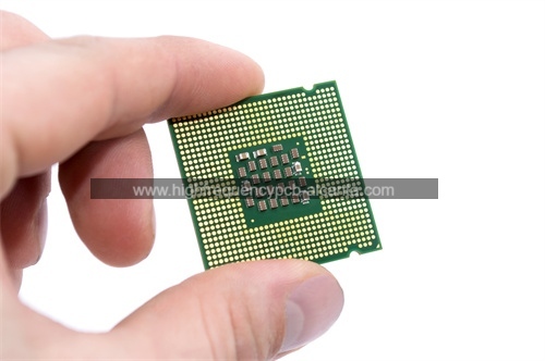
RF Cavities PCB Manufacturer
RF Cavities PCB Manufacturer,RF Cavities PCBs are specialized circuit boards designed for high-frequency applications involving radio frequency (RF) signals. These PCBs incorporate cavity structures within the substrate to create resonant chambers that enhance signal performance and reduce signal loss. The cavities are precisely engineered to optimize impedance and minimize interference, making them ideal for applications such as RF filters, oscillators, and antennas. Typically made from materials with low dielectric loss and high-frequency laminates, RF cavities PCBs ensure excellent signal integrity and efficient signal handling. Their advanced design supports high-frequency performance and reliability in communication systems, radar, and other RF-based technologies.
What is RF Cavities PCB?
RF Cavities PCBs (Radio Frequency Cavity Printed Circuit Boards) are specialized PCBs designed to operate at high-frequency ranges typically used in radio frequency (RF) applications. These PCBs are engineered with specific structures known as cavities, which are hollow or partially hollow sections within the board. These cavities serve to contain and guide RF signals with minimal interference and signal loss.
One of the primary purposes of RF Cavities PCBs is to enhance signal integrity and performance in high-frequency applications. By incorporating cavities, these PCBs can effectively manage electromagnetic interference (EMI) and crosstalk, which are common issues in RF circuits. This design helps maintain the quality and strength of RF signals, which is crucial for applications such as wireless communication, radar systems, and satellite communications.
The construction of RF Cavities PCBs involves the use of specialized materials and techniques. High-frequency laminates, such as PTFE (polytetrafluoroethylene) and Rogers materials, are often used due to their low dielectric loss and stable dielectric constant. These materials ensure minimal signal attenuation and phase distortion, which are critical for maintaining signal integrity at high frequencies.
Manufacturing RF Cavities PCBs requires precision and expertise. The process involves meticulous design and fabrication steps to create the cavities and ensure proper alignment and connectivity of the RF components. Advanced fabrication techniques, such as laser drilling and precision milling, are employed to create the cavities with high accuracy.
RF Cavities PCBs are widely used in various high-frequency applications across different industries. In telecommunications, they play a crucial role in the design of base stations, antennas, and RF modules. In aerospace and defense, these PCBs are used in radar systems, electronic warfare, and communication systems. The medical field also utilizes RF Cavities PCBs in imaging equipment and diagnostic devices that rely on high-frequency signals for accurate performance.
Overall, RF Cavities PCBs are essential for ensuring reliable and efficient operation in high-frequency applications. Their specialized design and construction enable the effective management of RF signals, making them a critical component in modern RF and microwave technology.
RF Cavities PCB Manufacturer
What are the RF Cavities PCB Design Guidelines?
Designing RF Cavities PCBs (Radio Frequency Cavity Printed Circuit Boards) involves adhering to specific guidelines to ensure optimal performance in high-frequency applications. Here are the key design guidelines for RF Cavities PCBs:
- Cavity Design and Geometry:The design of the cavities is crucial for effective signal management. The shape, size, and placement of cavities should be carefully calculated based on the operating frequency and desired performance. Cavity dimensions should be optimized to resonate at the desired frequency, minimizing losses and ensuring efficient signal propagation.
- Material Selection: High-frequency laminates are essential for minimizing signal loss and maintaining performance. Materials like PTFE (polytetrafluoroethylene) and Rogers substrates are commonly used due to their low dielectric loss and stable dielectric constant. The choice of material should match the frequency requirements and desired electrical performance.
- Impedance Matching: Proper impedance matching is critical for minimizing reflections and signal loss. The PCB design should include impedance-controlled traces and carefully designed transmission lines to ensure impedance consistency throughout the circuit.
- Minimize Losses and Interference: RF Cavities PCBs should be designed to minimize electromagnetic interference (EMI) and crosstalk. This involves using shielding techniques, proper grounding, and careful layout of signal paths to reduce unwanted interactions between signals.
- Thermal Management: High-frequency applications can generate significant heat. Effective thermal management is essential to prevent overheating and maintain circuit performance. This may involve incorporating thermal vias, heat sinks, or other cooling methods to dissipate heat effectively.
- Manufacturing Precision: The fabrication of RF Cavities PCBs requires high precision to ensure accurate cavity dimensions and alignment. Advanced manufacturing techniques, such as laser drilling and precision milling, should be used to achieve the required accuracy.
- Simulation and Testing: Before finalizing the design, simulations using electromagnetic analysis tools can help predict performance and identify potential issues. Post-manufacturing testing is also crucial to verify that the cavities and overall PCB meet design specifications and perform as expected in real-world conditions.
- Component Placement and Routing: The placement of components and routing of traces should be optimized to reduce signal path lengths and minimize interference. Critical RF components should be placed strategically, and traces should be routed to avoid sharp bends and unnecessary length.
- Grounding and Decoupling: Effective grounding and decoupling techniques are essential for maintaining signal integrity. Ensure proper grounding of cavities and RF components to reduce noise and improve overall performance.
By following these guidelines, designers can create RF Cavities PCBs that deliver reliable and high-performance results in demanding high-frequency applications.
What is the RF Cavities PCB Fabrication Process?
The fabrication process for RF Cavities PCBs (Radio Frequency Cavity Printed Circuit Boards) involves several specialized steps to ensure high performance and accuracy in high-frequency applications. Here is an overview of the RF Cavities PCB fabrication process:
- Design and Layout: The fabrication process begins with detailed design and layout of the RF Cavities PCB. This includes defining the cavity shapes, sizes, and positions based on the desired frequency and performance requirements. Advanced CAD software is used to create precise designs, including impedance-controlled traces and cavity dimensions.
- Material Selection and Preparation: High-frequency laminates, such as PTFE (polytetrafluoroethylene) or Rogers materials, are selected for their low dielectric loss and stable electrical properties. The laminate is prepared and cut to the required dimensions before moving on to the next fabrication steps.
- Drilling and Cavity Formation: Precision drilling is used to create the cavities in the PCB. Techniques such as laser drilling or mechanical milling are employed to achieve the exact dimensions and locations of the cavities. This step is crucial for ensuring that the cavities are accurately formed to match the design specifications.
- Copper Layer Deposition: A thin layer of copper is deposited onto the laminate using processes like chemical vapor deposition (CVD) or electroplating. This copper layer forms the conductive traces and pads required for the PCB’s circuitry.
- Etching and Patterning: The copper layer is then patterned using a photolithographic process. A photoresist is applied to the copper surface, and UV light is used to expose the photoresist in the desired trace patterns. The unexposed photoresist is removed, and the exposed copper is etched away to leave behind the circuitry.
- Cavity Etching and Formation: In addition to drilling, further etching may be required to refine the cavity shapes and ensure precise dimensions. This step may involve chemical etching or other techniques to achieve the final cavity profiles.
- Layer Lamination: For multilayer RF Cavities PCBs, multiple layers of laminate are stacked and bonded together using a lamination process. This involves applying heat and pressure to fuse the layers, creating a solid and reliable structure.
- Surface Finish: A surface finish is applied to protect the copper traces and enhance solderability. Common finishes include electroless nickel/immersion gold (ENIG), immersion silver, or other suitable coatings.
- Inspection and Testing: After fabrication, the PCB undergoes rigorous inspection and testing. This includes visual inspections, electrical testing, and performance verification to ensure that the RF cavities and overall circuitry meet design specifications and operate correctly at the desired frequencies.
- Cutting and Routing: The fabricated PCB is cut to its final shape and size. Additional routing may be performed to create specific cutouts or features as required by the design.
- Assembly: Once the PCB is complete, components are assembled onto the board. This may involve soldering, bonding, or other mounting techniques, depending on the component types and the design requirements.
- Final Testing and Quality Control: The assembled PCB undergoes final testing to ensure all components are functioning correctly and that the board meets performance standards. Quality control checks are performed to verify the overall reliability and consistency of the finished product.
By following these steps, manufacturers can produce RF Cavities PCBs that deliver high performance and accuracy for demanding high-frequency applications.
How Do You Manufacture RF Cavities PCB?
Manufacturing RF Cavities PCBs (Radio Frequency Cavity Printed Circuit Boards) involves a series of precise and specialized steps to ensure the effective handling of high-frequency signals and minimal signal loss. Here is an overview of the manufacturing process:
- Design and Planning: The process begins with detailed design work, which includes defining the RF cavity shapes, sizes, and locations based on the specific frequency and performance requirements. Design software is used to create detailed layouts and schematics that guide the manufacturing process.
- Material Selection:High-frequency laminates such as PTFE (polytetrafluoroethylene), Rogers, or other specialized materials are selected for their low dielectric loss and high-frequency performance. These materials are prepared and cut to the required dimensions for the PCB layers.
- Layer Preparation: The laminate material is processed to create the individual layers of the PCB. For multilayer designs, the layers are prepared separately before being assembled. This preparation includes cutting the laminate to size and applying a thin copper layer to one or both sides.
- Drilling and Cavity Formation: Precision drilling or laser cutting is used to create the cavities within the PCB. These cavities are designed to control and guide RF signals, and their dimensions must be accurate to ensure optimal performance. Laser drilling or mechanical milling is employed to achieve the required cavity shapes and sizes.
- Copper Deposition:A layer of copper is deposited onto the laminate using techniques like chemical vapor deposition (CVD) or electroplating. This copper layer forms the conductive traces and pads needed for the PCB’s circuitry.
- Photoresist Application and Etching: A photoresist layer is applied to the copper surface, and UV light is used to expose specific areas according to the design pattern. The unexposed photoresist is removed, and the exposed copper is etched away, leaving behind the desired circuitry and cavity structures.
- Cavity Refinement:Additional etching or milling may be performed to refine the cavity shapes and ensure precise dimensions. This step is crucial for achieving the correct cavity profiles and ensuring the RF performance of the PCB.
- Layer Lamination: For multilayer PCBs, the prepared layers are stacked and bonded together using a lamination process. Heat and pressure are applied to fuse the layers, creating a solid and cohesive structure. This step ensures that all layers are properly aligned and adhered.
- Surface Finishing:A surface finish is applied to protect the copper traces and improve solderability. Common finishes include electroless nickel/immersion gold (ENIG), immersion silver, or other suitable coatings.
- Inspection and Testing: After the initial fabrication, the PCB undergoes thorough inspection and testing. This includes visual inspections to check for defects, electrical tests to ensure functionality, and performance tests to verify that the RF cavities and circuitry meet design specifications.
- Cutting and Routing: The PCB is cut to its final shape and size, and any additional routing or cutouts required by the design are performed. This step ensures that the board meets the final specifications and can fit into its intended application.
- Component Assembly: Components are assembled onto the PCB using various techniques such as soldering, bonding, or surface-mount technology (SMT). This step involves placing and securing components according to the design requirements.
- Final Testing and Quality Control: The assembled PCB undergoes final testing to ensure that all components are functioning correctly and that the board meets performance and quality standards. Quality control checks are performed to ensure the reliability and consistency of the finished product.
By following these steps, manufacturers can produce RF Cavities PCBs that offer high performance and reliability for high-frequency applications, ensuring effective signal management and minimal interference.
How Much Should RF Cavities PCB Cost?
The cost of RF Cavities PCBs (Radio Frequency Cavity Printed Circuit Boards) can vary widely depending on several factors. Here’s an overview of the key elements that influence the cost:
- Design Complexity:The complexity of the PCB design, including the number and shape of cavities, impacts the cost. More intricate designs with precise cavity dimensions and advanced features will generally be more expensive to manufacture.
- Material Selection:High-frequency laminates such as PTFE (polytetrafluoroethylene) or Rogers materials are typically more expensive than standard PCB materials. The choice of material affects both the base cost and the performance characteristics of the PCB.
- Layer Count: The number of layers in the PCB affects the cost. Multilayer PCBs, which are common in high-frequency applications, require additional manufacturing processes and materials, increasing the overall cost.
- Cavity Formation: The methods used for creating cavities, such as laser drilling or precision milling, influence the cost. High-precision techniques are often more expensive due to the equipment and expertise required.
- Quantity: Production volume plays a significant role in cost. Larger quantities generally benefit from economies of scale, reducing the per-unit cost. Conversely, small batch or prototype runs tend to have higher per-unit costs due to setup and tooling expenses.
- Surface Finish:The type of surface finish applied to the PCB, such as ENIG (Electroless Nickel/Immersion Gold) or other high-end finishes, can impact the cost. Specialty finishes that offer better performance or durability are typically more expensive.
- Testing and Inspection:Thorough testing and inspection processes add to the cost. High-frequency PCBs often require detailed performance testing to ensure signal integrity and reliability, which can contribute to higher overall costs.
- Fabrication and Assembly: The complexity of the fabrication and assembly processes, including additional steps like layer lamination or advanced component mounting, can affect the cost. More complex assemblies or additional processing steps will generally increase the price.
- Lead Time: Expedited production or tight deadlines can increase costs. Standard lead times are generally less expensive compared to rush orders or expedited production schedules.
- Vendor and Location: The cost can vary based on the manufacturer or vendor, as well as their geographic location. Different regions may have varying labor and material costs, influencing the final price.
For accurate pricing, it’s advisable to request quotes from PCB manufacturers with details on the design, material requirements, and production volume. This will provide a more tailored estimate based on your specific needs.
What is RF Cavities PCB Base Material?
The base material for RF Cavities PCBs (Radio Frequency Cavity Printed Circuit Boards) is critical to achieving high performance in high-frequency applications. The choice of base material impacts the PCB’s signal integrity, performance, and overall reliability. Here’s an overview of the key base materials commonly used for RF Cavities PCBs:
- PTFE (Polytetrafluoroethylene): PTFE is a widely used material for RF applications due to its excellent electrical properties. It has a low dielectric constant (typically around 2.1) and low dielectric loss, which makes it ideal for minimizing signal attenuation and distortion at high frequencies. PTFE-based laminates, such as those from Rogers Corporation, are popular choices for RF Cavities PCBs.
- Rogers Materials: Rogers offers a range of high-frequency laminate materials specifically designed for RF applications. Popular materials include Rogers RO4000 series and RO3000 series. These materials provide stable dielectric constants and low loss characteristics, making them suitable for high-performance RF Cavities PCBs.
- Ceramic-Based Laminates: Ceramic materials are sometimes used as base materials for RF PCBs due to their high dielectric constant and low loss. They offer excellent thermal stability and electrical performance, but they can be more expensive and harder to process compared to other materials.
- FR-4 with High-Frequency Modifications: While FR-4 is a standard material used in many PCBs, it can be modified for high-frequency applications with additional treatments or coatings. However, it generally does not perform as well as specialized high-frequency materials like PTFE or Rogers laminates in very high-frequency applications.
- Polyimide: Polyimide is another material used in RF applications, known for its high thermal stability and flexibility. It has a higher dielectric constant compared to PTFE but can be used in applications where thermal performance is critical.
- Liquid Crystal Polymer (LCP): LCPs are used in high-frequency applications for their low dielectric constant and low loss characteristics. They offer good signal integrity and thermal stability but can be more costly compared to other materials.
- Hybrid Laminates: In some cases, hybrid laminates that combine different materials may be used to achieve desired performance characteristics. For example, a laminate might use a combination of PTFE and ceramic fillers to balance cost and performance.
By selecting the appropriate base material, manufacturers can ensure that RF Cavities PCBs perform effectively in high-frequency environments, delivering reliable signal integrity and minimal interference.
Which Company Makes RF Cavities PCB?
Currently, there are many companies manufacturing RF Cavities PCBs (Radio Frequency Cavity Printed Circuit Boards) in the market, including Rogers Corporation, Taconic, Heraeus, SIKO, and Wanshih Electronic Co., Ltd. These companies possess advanced technology and equipment to produce high-performance RF Cavities PCBs, which are widely used in wireless communication, satellite communication, radar systems, and other fields.
Rogers Corporation is renowned for its advanced high-frequency materials, with its RO4003C and RO4350B materials widely applied in the RF field. Taconic is well-known for its high-frequency microwave materials, which are extensively used in communication and radar systems. Heraeus focuses on the development of high thermal conductivity and high-frequency materials, providing excellent solutions for high-frequency PCBs. SIKO and Wanshih Electronic also have extensive experience in the manufacturing and processing of high-frequency PCBs, offering high-quality RF Cavities PCB products.
Our company also has the capability to manufacture RF Cavities PCBs. Our products use high-performance base materials to ensure excellent performance under high-frequency conditions. Our RF Cavities PCB products have the following features:
- Superior High-Frequency Performance: We use high-quality high-frequency base materials, such as Rogers and Taconic, to ensure stability and low loss under high-frequency conditions.
- High Precision Processing: Our company has advanced processing equipment and technical teams capable of high-precision circuit processing and lamination, ensuring high product quality.
- Multilayer Structure Design: We can design and manufacture multilayer RF Cavities PCBs according to customer needs, meeting the requirements of complex circuits.
- Excellent After-Sales Service: We offer comprehensive after-sales service to ensure customers receive timely technical support and solutions during use.
- Customized Services: We can provide customized RF Cavities PCB design and manufacturing services based on specific customer requirements, ensuring that the products fully meet application needs.
Through continuous technological innovation and strict quality control, our RF Cavities PCB products have been widely recognized in the market and are used in various high-frequency applications such as communication, radar, and satellites. If you have RF Cavities PCB needs, please feel free to contact us. We are dedicated to providing you with high-quality products and services.
In summary, whether it is from material selection, processing technology, or after-sales service, our company is capable of producing high-quality RF Cavities PCBs to meet the demands of various high-frequency applications.
What are the 7 Qualities of Good Customer Service?
Good customer service is essential for building strong relationships with customers and ensuring their satisfaction. Here are seven key qualities that define excellent customer service:
- Responsiveness: Timely and effective responses to customer inquiries and issues are crucial. Good customer service involves addressing questions, concerns, or problems quickly, minimizing wait times, and providing clear and concise answers.
- Empathy: Demonstrating understanding and empathy towards customers’ needs and feelings helps build trust and rapport. Empathetic service involves actively listening to customers, acknowledging their concerns, and showing genuine care and consideration for their situations.
- Professionalism: Maintaining a high standard of professionalism is important in all customer interactions. This includes being courteous, respectful, and knowledgeable. Professionalism also involves handling situations calmly and effectively, regardless of the circumstances.
- Consistency: Providing a consistent level of service ensures that customers have a reliable experience every time they interact with your business. Consistency involves applying the same standards of service and quality across all interactions and channels.
- Problem-Solving Skills: Effective customer service representatives are adept at solving problems and finding solutions. This involves understanding the root cause of issues, thinking critically, and providing practical and satisfactory solutions to resolve customer concerns.
- Clear Communication: Good customer service requires clear and effective communication. This includes using simple and understandable language, avoiding jargon, and ensuring that information is conveyed accurately. Clear communication helps prevent misunderstandings and ensures that customers are well-informed.
- Proactivity: Anticipating and addressing customer needs before they arise shows a high level of service. Proactive customer service involves identifying potential issues, offering solutions or assistance before customers ask, and continuously improving service based on customer feedback.
By focusing on these qualities, businesses can enhance their customer service and create positive experiences that foster loyalty and satisfaction.
FAQs about RF Cavities PCB
What are RF Cavities PCBs used for?
RF Cavities PCBs are used in high-frequency applications such as communication systems, radar, and other RF technologies.
What materials are best for RF Cavities PCBs?
High-frequency dielectric materials like PTFE or ceramic are preferred for RF Cavities PCBs.
How do I choose the right RF Cavities PCB manufacturer?
Consider factors such as the manufacturer’s experience with RF technologies, the quality of their materials, and their ability to meet your specific design requirements.
What is the lead time for RF Cavities PCB fabrication?
Lead time can vary based on the complexity of the design and the manufacturer’s capacity, but it is typically several weeks.
How can I reduce costs for RF Cavities PCBs?
Optimizing your design for manufacturability, ordering in larger quantities, and selecting cost-effective materials can help reduce costs.