 Professional high frequency circuit board supplier
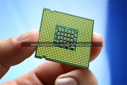
What is QFN Package?
QFN Package Manufacturer,QFN (Quad Flat No-Lead) package is a compact and versatile semiconductor packaging solution known for its low profile and excellent thermal performance. Featuring a flat body with leads on all four sides, QFN packages provide efficient heat dissipation and reliable electrical connections. They support high-density integration of chips, enabling miniaturization in electronic assemblies. Widely used in consumer electronics, automotive, and telecommunications industries, QFN packages ensure optimal performance in space-constrained environments. With their precise construction and compatibility with surface-mount assembly processes, QFN packages offer a reliable and cost-effective solution for various electronic designs requiring compactness and thermal efficiency.
QFN stands for Quad Flat No-Lead, which is a type of surface-mount package used for integrated circuits. The QFN package is characterized by its flat, square shape with leads on all four sides of the package. However, unlike traditional leaded packages, QFN packages do not have leads extending from the package body. Instead, the electrical connections are made via exposed metal pads on the bottom of the package, which are soldered directly to the printed circuit board (PCB).
QFN packages offer several advantages, including a small footprint, excellent thermal performance due to the large exposed thermal pad on the bottom, and good electrical performance at high frequencies. These characteristics make QFN packages popular choices for a wide range of applications, including consumer electronics, telecommunications, automotive, and industrial devices.
QFN Package Manufacturer
What are the Functions of QFN Package?
The QFN (Quad Flat No-Lead) package serves several functions in the context of integrated circuits and electronic devices:
Encapsulation and Protection: One of the primary functions of the QFN package is to encapsulate and protect the integrated circuit (IC) from external environmental factors such as moisture, dust, and mechanical damage. The package helps ensure the integrity and reliability of the IC.
Electrical Connection: The QFN package provides electrical connections between the integrated circuit and the printed circuit board (PCB). This is achieved through the exposed metal pads on the bottom of the package, which are soldered directly onto the PCB.
Heat Dissipation: QFN packages often feature a large exposed thermal pad on the bottom, which enhances heat dissipation from the integrated circuit. This helps to regulate the temperature of the IC during operation, preventing overheating and ensuring optimal performance and reliability.
Miniaturization: QFN packages are known for their small footprint and low profile, making them ideal for applications where space is limited. The compact size of QFN packages allows for higher component density on PCBs, enabling the design of smaller and more compact electronic devices.
High-Frequency Performance: Due to their compact design and short electrical paths, QFN packages offer excellent high-frequency performance. This makes them suitable for applications requiring fast signal propagation and high-speed data transmission, such as wireless communication and digital signal processing.
Ease of Manufacturing: QFN packages are typically compatible with standard surface-mount technology (SMT) assembly processes, making them easy and cost-effective to manufacture in large volumes. The absence of leads simplifies the assembly process and reduces the risk of solder joint failures.
Overall, the QFN package plays a crucial role in providing electrical connectivity, protection, thermal management, and miniaturization for integrated circuits, contributing to the functionality, performance, and reliability of electronic devices.
What are the Different Types of QFN Package?
There are several variations of QFN (Quad Flat No-Lead) packages, each with its own design features and characteristics. Some of the common types of QFN packages include:
Thin QFN (TQFN): Thin QFN packages have a reduced overall height compared to standard QFN packages, making them suitable for applications where space constraints are critical. They typically have a thinner profile while maintaining the same footprint as standard QFN packages.
Micro QFN (uQFN): Micro QFN packages are even smaller than standard QFN packages, with reduced dimensions in terms of both footprint and height. They are designed for ultra-compact electronic devices where miniaturization is paramount.
Dual QFN (DQFN): Dual QFN packages feature two separate sets of electrical connections on opposite sides of the package, providing additional flexibility for routing signals and power distribution. They are often used in applications requiring higher pin counts or complex signal routing.
Quad Flat No-Lead Enhanced (QFN-EP): QFN-EP packages feature an extended exposed pad on the bottom of the package, which enhances thermal dissipation and improves solder joint reliability. They are suitable for applications requiring efficient heat management and high reliability.
Power QFN (PQFN): Power QFN packages are designed to handle higher power levels and offer improved thermal performance compared to standard QFN packages. They often feature larger exposed thermal pads and heavier copper traces to dissipate heat more effectively.
Quad Flat No-Lead Very Thin Package (QFN-VT): QFN-VT packages are ultra-thin variants of QFN packages, typically with a height of less than 0.5 mm. They are used in applications where height constraints are extremely tight, such as mobile devices and wearables.
These are just a few examples of the various types of QFN packages available in the market. Each type offers specific advantages and is chosen based on the requirements of the application, such as size constraints, thermal performance, pin count, and power handling capabilities.
How does QFN Package Relate to IC Packaging?
The QFN (Quad Flat No-Lead) package is a type of integrated circuit (IC) packaging. IC packaging refers to the process of enclosing an integrated circuit in a protective housing or package, which serves several functions such as providing electrical connections, mechanical support, thermal management, and environmental protection.
QFN packages are a popular choice for IC packaging due to their compact size, excellent thermal performance, and ease of manufacturing. They belong to the category of surface-mount packages, meaning that the electrical connections between the IC and the printed circuit board (PCB) are made via exposed metal pads on the bottom of the package, which are soldered directly onto the PCB.
In terms of IC packaging, QFN packages provide the following:
Electrical Connections: QFN packages offer electrical connections between the integrated circuit and the PCB. The exposed metal pads on the bottom of the package serve as terminals for soldering to the PCB, allowing for reliable electrical connections.
Thermal Management: QFN packages typically feature a large exposed thermal pad on the bottom, which helps dissipate heat generated by the integrated circuit during operation. This enhances thermal performance and prevents overheating, ensuring the reliability and longevity of the IC.
Mechanical Support: The QFN package provides mechanical support and protection for the integrated circuit, shielding it from physical damage, moisture, and other environmental factors. The package helps ensure the integrity and reliability of the IC in various operating conditions.
Miniaturization: QFN packages are known for their small footprint and low profile, making them suitable for applications where space is limited. They enable the design of compact electronic devices with high component density on PCBs, contributing to miniaturization and form factor reduction.
Overall, QFN packages play a significant role in IC packaging by providing electrical connectivity, thermal management, mechanical support, and miniaturization for integrated circuits, thereby enhancing their functionality, performance, and reliability in electronic devices.
What are the Differences Between QFN Package and PCB?
QFN Package and PCB (Printed Circuit Board) are two distinct components in electronic systems, each serving different purposes. Here are the key differences between them:
Function:
QFN Package: The QFN package is a housing for integrated circuits (ICs). It provides electrical connections, thermal management, and physical protection for the IC.
PCB: The PCB is a board made of insulating material (like fiberglass) with conductive pathways etched or printed onto its surface. It provides a platform for mounting and interconnecting electronic components, including ICs, resistors, capacitors, and others.
Construction:
QFN Package: QFN packages are typically made of plastic or ceramic materials and feature a flat, square shape with metal pads on the bottom for electrical connections.
PCB: PCBs are made of layers of insulating substrate with conductive traces (usually copper) laminated onto them. Components are soldered onto the PCB, and the traces provide electrical pathways between them.
Size and Shape:
QFN Package: QFN packages come in various sizes and shapes, but they are generally flat and compact, with leads on all four sides or sometimes on just two opposite sides.
PCB: PCBs vary in size and shape according to the requirements of the electronic device they are part of. They can be rectangular, circular, or irregularly shaped, depending on the application.
Functionality:
QFN Package: QFN packages primarily serve to house and protect ICs while providing electrical connections and managing heat dissipation.
PCB: PCBs serve as a platform for mounting and interconnecting various electronic components to create functional circuits. They provide electrical pathways for signal transmission and power distribution.
Interconnection:
QFN Package: QFN packages are mounted onto the PCB and soldered directly onto the copper pads on the board’s surface.
PCB: PCBs provide the interconnection between electronic components by means of conductive traces, vias, and solder joints.
Manufacturing:
QFN Package: QFN packages are manufactured separately from PCBs and are typically produced in specialized semiconductor packaging facilities.
PCB: PCBs are fabricated separately from components and are manufactured in specialized PCB manufacturing facilities using processes such as etching, drilling, and soldering.
In summary, while both QFN packages and PCBs are essential components in electronic systems, they serve different functions and have distinct characteristics in terms of construction, size, shape, functionality, interconnection, and manufacturing processes.
What are the Main Structures and Production Technologies of QFN Package?
The main structures and production technologies of QFN (Quad Flat No-Lead) packages involve several key elements and processes:
Package Body: The package body of a QFN package is typically made of plastic or ceramic material. It provides structural support and protection for the integrated circuit (IC) housed within it. The package body is often designed with a flat, square shape, although variations in shape and size are possible.
Exposed Thermal Pad: One of the distinctive features of QFN packages is the exposed thermal pad located on the bottom side of the package. This pad serves as a heat sink, allowing efficient dissipation of heat generated by the IC during operation. The exposed thermal pad is crucial for managing thermal performance and ensuring the reliability of the IC.
Leadframe or Substrate: QFN packages are constructed using either a leadframe or a substrate as the base material. The leadframe or substrate provides the foundation for mounting the IC and creating electrical connections. Leadframes are typically made of metal and are stamped or etched to form the desired shape, while substrates are made of insulating material such as ceramic or laminate and feature conductive traces for interconnection.
Die Attach: The IC chip (die) is attached to the leadframe or substrate using die attach materials such as epoxy or solder. This process involves precise placement and alignment of the IC chip onto the designated area of the leadframe or substrate.
Wire Bonding: Electrical connections between the IC chip and the leadframe or substrate are established using wire bonding techniques. Thin metal wires (typically gold or aluminum) are bonded from the bonding pads on the IC chip to the corresponding pads on the leadframe or substrate.
Mold Compound Encapsulation: Once the die attach and wire bonding processes are completed, the entire assembly is encapsulated in a mold compound. The mold compound provides environmental protection, mechanical support, and insulation for the IC. It is molded around the assembly and cured to form the final package body.
Surface Finishing: The exposed metal pads on the bottom side of the QFN package undergo surface finishing processes to enhance solderability and ensure reliable electrical connections with the printed circuit board (PCB). Common surface finishes include tin-lead (SnPb), lead-free solder (e.g., SAC), and gold plating.
Singulation: After encapsulation, the QFN packages are typically formed into arrays on a panel and then singulated into individual units using processes such as sawing or laser cutting. This results in separate QFN packages ready for assembly onto PCBs.
Overall, the production technologies of QFN packages involve a series of precise manufacturing steps to create a reliable and efficient housing for integrated circuits, with a focus on thermal management, electrical connectivity, and environmental protection.
Frequently Asked Questions (FAQs)
What does QFN stand for?
QFN stands for Quad Flat No-Lead. It is a type of surface-mount integrated circuit package characterized by its flat, square shape and leads on all four sides of the package.
What are the advantages of QFN packages?
QFN packages offer several advantages, including small footprint, excellent thermal performance, good electrical performance at high frequencies, ease of manufacturing, and compatibility with surface-mount assembly processes.
What are the applications of QFN packages?
QFN packages are used in a wide range of applications, including consumer electronics (e.g., smartphones, tablets), telecommunications, automotive electronics, industrial automation, medical devices, and more.
How are QFN packages mounted onto printed circuit boards (PCBs)?
QFN packages are mounted onto PCBs using surface-mount technology (SMT). The exposed metal pads on the bottom of the QFN package are soldered directly onto the copper pads on the PCB.
What are some common variations of QFN packages?
Common variations of QFN packages include Thin QFN (TQFN), Micro QFN (uQFN), Dual QFN (DQFN), Quad Flat No-Lead Enhanced (QFN-EP), Power QFN (PQFN), and Quad Flat No-Lead Very Thin Package (QFN-VT).
How are QFN packages manufactured?
The manufacturing process of QFN packages involves several key steps, including die attach, wire bonding, mold compound encapsulation, surface finishing, singulation, and quality testing. These processes are carried out in specialized semiconductor packaging facilities.
What are some considerations for designing with QFN packages?
When designing with QFN packages, engineers need to consider factors such as thermal management, pad layout, soldering techniques, signal integrity, and manufacturability to ensure optimal performance and reliability of the electronic device.
Are there any reliability concerns with QFN packages?
While QFN packages offer many advantages, proper design and manufacturing practices are essential to mitigate potential reliability concerns such as solder joint cracking, package warpage, and thermal stress. Adhering to industry standards and guidelines can help ensure the reliability of QFN-based designs.
Conclusion
In conclusion, the QFN (Quad Flat No-Lead) package is a versatile and widely used type of integrated circuit packaging. Its flat, square shape and leads on all four sides make it suitable for a variety of applications across industries such as consumer electronics, telecommunications, automotive, and more.
QFN packages offer numerous advantages, including small footprint, excellent thermal performance, good electrical performance at high frequencies, ease of manufacturing, and compatibility with surface-mount assembly processes. These qualities make them ideal for modern electronic devices where space, performance, and reliability are crucial considerations.
The production technologies of QFN packages involve several key processes, including die attach, wire bonding, mold compound encapsulation, surface finishing, and singulation. These processes are carried out in specialized semiconductor packaging facilities to create reliable and efficient housing for integrated circuits.
When designing with QFN packages, engineers need to consider factors such as thermal management, pad layout, soldering techniques, signal integrity, and manufacturability to ensure optimal performance and reliability of the electronic device.
Overall, QFN packages play a significant role in advancing the capabilities and functionality of electronic devices, contributing to innovations in various fields and driving progress in technology.


