 Professional high frequency circuit board supplier
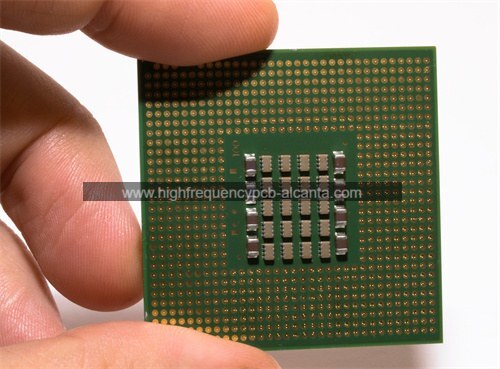
What is POP Package Substrate?
POP Package Substrate Manufacturer,POP (Package on Package) substrate enables vertical integration of semiconductor packages, optimizing space and performance. It features stacked chips, minimizing interconnect length and enhancing signal speed. POP substrates ensure reliable electrical connections and efficient thermal management, critical for high-density applications like mobile devices and gaming consoles. They offer compact designs, reducing overall system footprint while maintaining robust mechanical support. Widely used in consumer electronics, POP package substrates enable the development of compact and powerful devices. Their innovative design and advanced materials facilitate seamless integration of multiple components, ensuring superior performance and reliability in modern electronic systems.
POP (Package on Package) substrate is a type of substrate used in integrated circuit packaging technology. In a POP configuration, two or more integrated circuit packages are stacked vertically on top of each other, with the top package mounted directly on top of the bottom package. The substrate serves as the interface between the packages, providing electrical connections between them.
POP substrates typically consist of a thin, flat piece of material, such as a laminate or a ceramic, with metal traces and vias (vertical interconnect access) etched or deposited onto its surface. These traces and vias route signals and power between the different packages in the stack, enabling them to communicate and work together as a single integrated system.
The use of POP packaging allows for increased functionality and performance in a smaller form factor, making it a popular choice for mobile devices and other space-constrained applications. Additionally, POP substrates can help to improve thermal management and signal integrity by reducing the length of interconnects between packages.
POP Package Substrate Manufacturer
What are the functions of POP Package Substrate?
The POP (Package on Package) substrate serves several important functions in integrated circuit packaging:
Electrical connections: The substrate provides a platform for connecting the various integrated circuit packages stacked on top of each other. It contains metal traces and vias that route signals, power, and ground between the packages, enabling them to communicate and work together effectively.
Mechanical support: The substrate acts as a mechanical support structure for the stacked packages, ensuring that they are securely held in place and aligned correctly. This helps to prevent damage to the packages and ensures reliable operation of the entire system.
Thermal management: The substrate can help to dissipate heat generated by the integrated circuit packages, thereby improving thermal performance and reliability. By providing a path for heat to flow away from the packages, the substrate helps to prevent overheating and prolongs the lifespan of the devices.
Signal integrity: The design and layout of the substrate traces and vias are optimized to minimize signal degradation and ensure high-speed signal integrity. This helps to maintain the quality of electrical signals transmitted between the integrated circuit packages, ensuring reliable data transmission and processing.
Overall, the POP package substrate plays a critical role in enabling the integration of multiple integrated circuit packages into a compact and efficient system, while also ensuring reliable performance in terms of electrical connectivity, mechanical stability, thermal management, and signal integrity.
What are the different types of POP Package Substrate?
There are several different types of POP (Package on Package) substrates, each designed to meet specific performance, cost, and application requirements. Some common types include:
Laminate substrates: Laminate substrates are made of layers of fiberglass or other dielectric materials bonded together with epoxy resin. They are typically used in cost-sensitive applications and offer good electrical performance, mechanical stability, and thermal management.
Ceramic substrates: Ceramic substrates are made of ceramic materials such as alumina or aluminum nitride. They offer excellent thermal conductivity and stability, making them well-suited for high-power applications or applications where thermal management is critical.
Flex substrates: Flex substrates are made of flexible materials such as polyimide or polyester. They are often used in applications where space constraints or mechanical flexibility are important, such as wearable devices or flexible displays.
Embedded substrates: Embedded substrates are integrated directly into the PCB (printed circuit board) or package substrate, rather than being a separate component. This can help to reduce the overall size and cost of the package, while also improving electrical performance and reliability.
High-density interconnect (HDI) substrates: HDI substrates use advanced manufacturing techniques to achieve higher density and finer pitch traces and vias. They are often used in high-performance or high-density applications, such as smartphones or high-speed data communication devices.
Each type of POP substrate has its own advantages and limitations, and the choice of substrate depends on factors such as performance requirements, cost constraints, and specific application needs.
What is the relationship between POP Package Substrate and IC packaging?
The relationship between POP (Package on Package) substrate and IC (Integrated Circuit) packaging is that POP substrate is a type of substrate used in the packaging of integrated circuits.
IC packaging involves the process of enclosing one or more integrated circuits in a protective housing or package. This package provides electrical connections, mechanical support, thermal management, and environmental protection for the integrated circuit.
POP packaging takes the concept of IC packaging a step further by stacking multiple IC packages vertically on top of each other. The POP substrate serves as the interface between the stacked packages, providing electrical connections between them and ensuring their mechanical stability.
In other words, POP packaging utilizes a specific type of substrate, the POP substrate, to enable the stacking of multiple IC packages. The substrate plays a critical role in facilitating communication and integration between the stacked packages, while also providing support, thermal management, and signal integrity.
Overall, POP package substrates are an integral part of the IC packaging process, particularly in applications where space efficiency and performance are critical, such as in mobile devices and other compact electronic devices.
How does POP Package Substrate differ from PCB?
POP (Package on Package) substrates and PCBs (Printed Circuit Boards) serve different purposes and have distinct characteristics. Here are some key differences between the two:
Function:
POP substrate: POP substrates primarily serve as a platform for connecting and stacking multiple integrated circuit packages vertically on top of each other. They provide electrical connections, mechanical support, thermal management, and signal integrity between the stacked packages.
PCB: PCBs serve as a foundation for mounting and interconnecting various electronic components, including integrated circuits, resistors, capacitors, and connectors. They provide electrical connections between components and support the overall functionality of electronic devices.
Construction:
POP substrate: POP substrates are typically thin, flat structures made of materials such as laminate, ceramic, or flexible materials. They may contain metal traces, vias, and other features designed to facilitate the connection and stacking of integrated circuit packages.
PCB: PCBs are typically thicker and more rigid than POP substrates. They consist of multiple layers of substrate material (e.g., fiberglass, epoxy resin) laminated together with copper traces and vias etched or deposited onto the surface to form electrical connections between components.
Application:
POP substrate: POP substrates are commonly used in applications where space efficiency and performance are critical, such as in mobile devices, tablets, and other compact electronic devices.
PCB: PCBs are used in a wide range of electronic devices and systems, including computers, smartphones, automotive electronics, industrial equipment, and consumer electronics.
Integration:
POP substrate: POP substrates are typically used in conjunction with integrated circuit packages, enabling the stacking of multiple packages to achieve higher levels of integration and functionality.
PCB: PCBs integrate various electronic components and subsystems into a single, cohesive platform, providing the foundation for the overall operation of electronic devices and systems.
Overall, while both POP substrates and PCBs play critical roles in electronic packaging and interconnection, they serve different functions and are optimized for different applications and requirements.
What are the structure and production technology of POP Package Substrate?
The structure and production technology of POP (Package on Package) substrate can vary depending on factors such as the type of substrate material (e.g., laminate, ceramic, flex), the requirements of the specific application, and the manufacturing processes used. However, here is a general overview of the structure and production technology of POP package substrates:
Structure:
Substrate material: POP substrates are typically made of materials such as laminate (e.g., fiberglass-reinforced epoxy), ceramic (e.g., alumina, aluminum nitride), or flexible materials (e.g., polyimide, polyester). The choice of substrate material depends on factors such as electrical performance, thermal management, mechanical stability, and cost.
Metal traces and vias: The substrate contains metal traces (conductive pathways) and vias (vertical interconnect access) that are etched or deposited onto the surface. These traces and vias provide electrical connections between the integrated circuit packages stacked on top of each other.
Dielectric layers: In multi-layer substrates, dielectric layers made of insulating materials are sandwiched between the metal layers to provide isolation and prevent electrical shorting between the traces.
Surface finish: The substrate may have a surface finish applied to improve solderability and ensure reliable bonding between the substrate and the integrated circuit packages.
Production technology:
Substrate fabrication: The substrate fabrication process starts with the preparation of the substrate material, which may involve cutting, laminating, or forming the material into the desired shape and size. For laminate substrates, layers of fiberglass and epoxy resin are laminated together and cured to form the substrate. For ceramic substrates, the ceramic material is shaped and fired to achieve the desired dimensions and properties.
Metal deposition and patterning: Metal traces and vias are formed on the substrate surface using processes such as physical vapor deposition (PVD), chemical vapor deposition (CVD), or screen printing. These metal layers are then patterned using photolithography and etching techniques to define the desired circuitry.
Dielectric layer deposition: In multi-layer substrates, dielectric layers are deposited or laminated onto the substrate surface between the metal layers. These dielectric layers provide insulation and define the vertical interconnects between the metal layers.
Surface finishing: The substrate may undergo surface finishing processes such as solder mask application, surface treatment, or plating to improve solderability and surface integrity.
Testing and inspection: The finished substrates undergo testing and inspection to ensure that they meet the required electrical, mechanical, and quality specifications.
Overall, the production technology of POP package substrates involves a combination of materials processing, metal deposition, patterning, and surface finishing techniques to achieve the desired structure and performance characteristics.
Frequently Asked Questions (FAQs)
What is a POP package substrate?
A POP package substrate is a type of substrate used in integrated circuit packaging technology. It facilitates the stacking of multiple integrated circuit packages vertically on top of each other, providing electrical connections, mechanical support, thermal management, and signal integrity between the stacked packages.
What are the advantages of using POP package substrates?
POP package substrates offer several advantages, including increased functionality and performance in a smaller form factor, improved thermal management, enhanced signal integrity, and reduced overall system footprint. They are particularly well-suited for space-constrained applications such as mobile devices and wearable electronics.
What materials are used to make POP package substrates?
POP package substrates can be made from various materials, including laminate (e.g., fiberglass-reinforced epoxy), ceramic (e.g., alumina, aluminum nitride), and flexible materials (e.g., polyimide, polyester). The choice of substrate material depends on factors such as electrical performance, thermal management, mechanical stability, and cost.
How are POP package substrates manufactured?
The manufacturing process for POP package substrates involves substrate fabrication, metal deposition and patterning, dielectric layer deposition, surface finishing, and testing and inspection. Substrate fabrication includes preparing the substrate material, forming metal traces and vias, depositing dielectric layers, applying surface finishes, and conducting quality testing and inspection to ensure that the substrates meet the required specifications.
What are the different types of POP package substrates?
There are several different types of POP package substrates, including laminate substrates, ceramic substrates, flexible substrates, embedded substrates, and high-density interconnect (HDI) substrates. Each type of substrate has its own advantages and limitations, and the choice depends on factors such as performance requirements, cost constraints, and specific application needs.
What are the applications of POP package substrates?
POP package substrates are commonly used in applications where space efficiency, performance, and integration are critical, such as mobile devices, tablets, smartphones, wearable electronics, and other compact electronic devices. They enable the stacking of multiple integrated circuit packages to achieve higher levels of functionality and performance in a smaller footprint.
Conclusion
In conclusion, POP (Package on Package) package substrates play a crucial role in integrated circuit packaging technology, enabling the stacking of multiple IC packages vertically on top of each other. These substrates provide electrical connections, mechanical support, thermal management, and signal integrity between the stacked packages. POP substrates can be made from various materials, including laminate, ceramic, and flexible materials, and are manufactured using processes such as substrate fabrication, metal deposition and patterning, dielectric layer deposition, surface finishing, and testing and inspection. The use of POP package substrates offers several advantages, including increased functionality and performance in a smaller form factor, improved thermal management, enhanced signal integrity, and reduced overall system footprint. POP package substrates find applications in a wide range of electronic devices, particularly in space-constrained applications such as mobile devices, smartphones, tablets, wearable electronics, and other compact electronic devices.