 Professional high frequency circuit board supplier
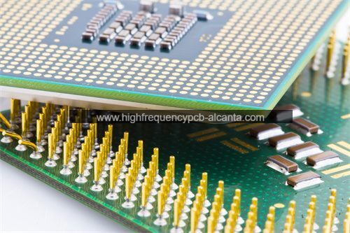
What is PGA Package Substrate?
PGA Package Substrate Manufacturer,PGA (Pin Grid Array) package substrate is a robust platform for semiconductor packaging, featuring a grid of pins for electrical connections. It offers reliable mechanical support and efficient signal transmission, ensuring stable performance in various applications. PGA substrates accommodate high-pin-count integrated circuits, facilitating complex electronic designs. With precise alignment and soldering, they ensure secure connections and signal integrity. PGA package substrates are commonly used in computing, networking, and telecommunications, where high-density interconnections are required. Their durable construction and compatibility with diverse components make PGA substrates essential for developing reliable electronic systems with superior performance and longevity.
PGA (Pin Grid Array) package substrate refers to the physical foundation upon which the pins of an integrated circuit (IC) package are arranged. PGA packages are characterized by having pins arranged in a uniform grid across the underside of the package, which corresponds to a matching grid of holes on the motherboard or other circuit board.
The substrate serves several functions:
Electrical Connections: The pins of the IC connect to the substrate, which in turn connects to the circuit board. This allows electrical signals to pass between the IC and the rest of the system.
Mechanical Support: The substrate provides structural support for the IC package, helping to protect it from physical damage.
Thermal Management: The substrate helps to dissipate heat generated by the IC, ensuring that it does not overheat and malfunction.
PGA packages were once very popular for CPUs and other high-performance integrated circuits, but they have largely been replaced by other package types such as Ball Grid Array (BGA) and Land Grid Array (LGA) due to their lower profile and better electrical performance. However, PGA packages are still used in some applications, particularly in legacy systems or for specialized components.
PGA Package Substrate Manufacturer
What are the Functions of PGA Package Substrate?
The PGA (Pin Grid Array) package substrate serves several important functions in electronic devices:
Electrical Connectivity: The primary function of the PGA package substrate is to provide a means for the electrical connections between the integrated circuit (IC) within the package and the rest of the system. The pins of the IC are connected to the substrate, which, in turn, connects to the circuit board or motherboard via solder joints or other methods. This enables the transmission of electrical signals between the IC and other components of the system.
Mechanical Support: The substrate provides structural support for the IC package. It helps to hold the IC securely in place and protects it from physical damage, such as bending or cracking. This mechanical support is crucial for maintaining the integrity of the IC and ensuring its proper functioning, especially in environments where the device may be subjected to mechanical stress.
Heat Dissipation: The substrate plays a role in dissipating heat generated by the IC during operation. Heat is conducted away from the IC through the substrate and into the surrounding environment or into a heat sink attached to the substrate. Effective heat dissipation is essential for preventing the IC from overheating, which can lead to performance degradation or even failure.
Electromagnetic Interference (EMI) Shielding: In some cases, the substrate may include features or materials that help to shield the IC from electromagnetic interference (EMI) generated by other components in the system or external sources. This can help to improve the overall electromagnetic compatibility (EMC) of the device and reduce the risk of interference-related issues.
Signal Integrity: The design and materials of the substrate can also influence the signal integrity of the electrical connections between the IC and the rest of the system. By minimizing signal degradation and distortion, the substrate helps to ensure reliable communication between the IC and other components, thereby maintaining the overall performance of the device.
Overall, the PGA package substrate plays a critical role in the functionality, reliability, and performance of electronic devices that utilize this packaging technology.
What are the Different Types of PGA Package Substrate?
There are several different types of PGA (Pin Grid Array) package substrates, each with its own characteristics and applications. Some common types include:
Ceramic Substrates: Ceramic substrates are often used in high-performance applications where reliability and thermal performance are critical. They offer excellent thermal conductivity, mechanical strength, and resistance to thermal and mechanical stresses. Ceramic substrates are typically more expensive than organic substrates but are preferred in applications such as microprocessors, memory modules, and high-frequency RF devices.
Organic Substrates: Organic substrates, typically made of materials like epoxy resin or fiberglass, are more commonly used in consumer electronics and lower-cost applications. They are less expensive than ceramic substrates but may have lower thermal conductivity and mechanical strength. Organic substrates are suitable for a wide range of applications, including CPUs, GPUs, memory chips, and other integrated circuits.
Multi-layer Substrates: Multi-layer substrates consist of multiple layers of material, often alternating between conductive and insulating layers. These substrates allow for more complex wiring configurations and improved signal integrity compared to single-layer substrates. Multi-layer substrates are commonly used in high-density applications where space is limited, such as mobile devices and networking equipment.
Flexible Substrates: Flexible substrates, typically made of materials like polyimide or polyester, are used in applications where flexibility or conformability is required. These substrates are lightweight, thin, and can be bent or shaped to fit into tight spaces. Flexible substrates are commonly used in wearable devices, flexible displays, and other applications where traditional rigid substrates are impractical.
Composite Substrates: Composite substrates combine different materials, such as ceramic and organic materials, to achieve a balance of performance and cost. These substrates may offer improved thermal conductivity and mechanical strength compared to organic substrates while being more cost-effective than ceramic substrates. Composite substrates are used in a variety of applications, including automotive electronics, industrial equipment, and telecommunications.
Overall, the choice of PGA package substrate depends on factors such as performance requirements, cost constraints, thermal management needs, and the specific application of the electronic device.
How does PGA Package Substrate Relate to IC Packaging?
PGA (Pin Grid Array) package substrate is a crucial component within the realm of integrated circuit (IC) packaging. IC packaging involves enclosing an integrated circuit (IC) die within a protective casing that provides electrical connections, mechanical support, and thermal management. PGA package substrate specifically refers to the physical foundation upon which the pins of an IC package are arranged in a grid pattern.
Here’s how PGA package substrate relates to IC packaging:
Electrical Connections: The substrate provides a platform for the IC’s pins to be attached, forming the electrical connections between the IC and the external environment, typically a printed circuit board (PCB) or motherboard. The substrate contains conductive pathways that facilitate the flow of electrical signals between the IC and other components.
Mechanical Support: The substrate serves as a mechanical foundation for the IC package, holding the IC securely in place and protecting it from physical damage. It helps to distribute mechanical stress and prevents the IC from bending or cracking, ensuring its integrity and reliability.
Heat Dissipation: The substrate aids in dissipating heat generated by the IC during operation. Heat is conducted away from the IC through the substrate and may be dissipated into the surrounding environment or transferred to a heat sink attached to the substrate. Effective thermal management is essential for preventing the IC from overheating, which can degrade performance or lead to failure.
Signal Integrity: The design and materials of the substrate can influence the signal integrity of the electrical connections between the IC and the rest of the system. Maintaining signal integrity is crucial for ensuring reliable communication between the IC and other components, which impacts the overall performance of the device.
In summary, the PGA package substrate is an integral part of IC packaging, providing electrical connectivity, mechanical support, thermal management, and signal integrity for the enclosed IC die. It plays a critical role in ensuring the functionality, reliability, and performance of electronic devices that utilize PGA packaging technology.
What are the Differences Between PGA Package Substrate and PCB?
PGA package substrate and PCB (Printed Circuit Board) are both essential components in electronic devices, but they serve different functions and have distinct characteristics. Here are the key differences between PGA package substrate and PCB:
Function:
PGA Package Substrate: The primary function of the PGA package substrate is to provide a platform for mounting the integrated circuit (IC) die and forming electrical connections between the IC and the external environment (such as a PCB). It also provides mechanical support, heat dissipation, and signal integrity for the enclosed IC.
PCB: The main function of a PCB is to provide a physical structure for mounting and interconnecting electronic components. It acts as a base for attaching components like ICs, resistors, capacitors, and connectors. PCBs facilitate electrical connections between components and provide a means for routing signals between them.
Design:
PGA Package Substrate: PGA substrates are typically smaller and designed specifically to accommodate a single IC package. They often feature a grid pattern of pins or pads where the IC’s pins are attached, and they may include layers of conductive and insulating materials for routing signals and managing heat.
PCB: PCBs come in various sizes and shapes and can accommodate multiple components arranged in different configurations. They are designed with layers of conductive traces and insulating layers (typically made of fiberglass-reinforced epoxy resin) that form the circuitry and provide mechanical support.
Components Attached:
PGA Package Substrate: PGA substrates primarily host a single IC package, providing the foundation for mounting and connecting the IC.
PCB: PCBs host a variety of electronic components, including ICs, resistors, capacitors, connectors, and other passive and active components. These components are soldered or mounted onto the PCB’s surface or within drilled holes.
Complexity:
PGA Package Substrate: PGA substrates tend to be less complex in design compared to PCBs. They are designed specifically for the requirements of a particular IC package and are optimized for electrical performance, heat dissipation, and mechanical support.
PCB: PCBs can vary greatly in complexity, depending on the specific application and the number and type of components they need to accommodate. They can range from simple single-layer boards to complex multi-layer boards with intricate circuitry.
In summary, while PGA package substrates and PCBs are both integral to electronic devices, they serve different functions and have distinct designs. PGA substrates focus on providing a platform for mounting and connecting IC packages, while PCBs provide a broader foundation for hosting a variety of electronic components and forming the overall circuitry of a device.
What are the Main Structures and Production Technologies of PGA Package Substrate?
The main structures and production technologies of PGA (Pin Grid Array) package substrates can vary depending on factors such as the specific application, performance requirements, and manufacturing capabilities. However, here are some common structures and production technologies used in PGA package substrate manufacturing:
Substrate Material:
Ceramic: Ceramic substrates offer excellent thermal conductivity, mechanical strength, and reliability. They are commonly used in high-performance applications where thermal management is critical.
Organic: Organic substrates, typically made of materials like epoxy resin or fiberglass, are more cost-effective than ceramic substrates but may have lower thermal conductivity and mechanical strength. They are commonly used in consumer electronics and lower-cost applications.
Layer Structure:
Single-layer: Simple PGA substrates may consist of a single layer of material with conductive traces and pads arranged in a grid pattern for attaching the IC’s pins.
Multi-layer: More complex PGA substrates may feature multiple layers of material, typically alternating between conductive and insulating layers. Multi-layer substrates allow for more complex wiring configurations and improved signal integrity.
Conductive Traces and Pads:
Conductive traces: These are pathways of conductive material (e.g., copper) that form the electrical connections between the IC’s pins and the external environment (e.g., a printed circuit board).
Pads: Pads are areas of conductive material where the IC’s pins are attached. They provide a surface for soldering or bonding the pins to the substrate.
Production Technologies:
Screen Printing: Screen printing is commonly used to deposit conductive materials (e.g., solder paste) onto the substrate surface to create conductive traces and pads.
Etching: Etching techniques may be used to selectively remove unwanted material from the substrate surface, leaving behind the desired conductive traces and patterns.
Laser Drilling: Laser drilling is often used to create holes in the substrate for attaching the IC’s pins or for through-hole plating in multi-layer substrates.
Solder Mask Application: Solder mask materials are applied to the substrate surface to protect the conductive traces and pads from oxidation and to define the areas where solder will be applied during assembly.
Plating: Plating processes are used to deposit thin layers of metal onto the substrate surface, enhancing conductivity and providing corrosion resistance.
Overall, the main structures and production technologies of PGA package substrates are tailored to meet the specific requirements of the application, ensuring reliable electrical connections, mechanical support, thermal management, and signal integrity for the enclosed IC.
Frequently Asked Questions (FAQs)
What is a PGA package substrate?
A PGA package substrate is the physical foundation upon which the pins of an integrated circuit (IC) package are arranged in a grid pattern. It provides electrical connections, mechanical support, thermal management, and signal integrity for the enclosed IC.
What are the main functions of a PGA package substrate?
The main functions of a PGA package substrate include providing electrical connectivity between the IC and the external environment, offering mechanical support to the IC package, dissipating heat generated by the IC, and maintaining signal integrity for reliable communication.
What are the different types of PGA package substrates?
PGA package substrates come in various types, including ceramic substrates, organic substrates, multi-layer substrates, flexible substrates, and composite substrates. Each type offers different characteristics and is suitable for specific applications.
How is a PGA package substrate different from a PCB?
While both PGA package substrates and PCBs (Printed Circuit Boards) are essential components in electronic devices, they serve different functions. PGA package substrates primarily provide a platform for mounting and connecting IC packages, while PCBs host a variety of electronic components and form the overall circuitry of a device.
What are the main production technologies used in manufacturing PGA package substrates?
Production technologies for PGA package substrates include screen printing, etching, laser drilling, solder mask application, plating, and others. These technologies are used to create conductive traces, pads, and other features on the substrate surface.
What are the advantages of PGA package substrates?
Advantages of PGA package substrates include high reliability, excellent thermal conductivity, good mechanical strength, and optimized electrical performance. They are suitable for high-performance applications where these characteristics are critical.
What are the typical applications of PGA package substrates?
PGA package substrates are commonly used in various applications, including microprocessors, memory modules, high-frequency RF devices, automotive electronics, industrial equipment, telecommunications, and more.
Conclusion
It seems you’re asking for a conclusion, but it’s not entirely clear what you’re referring to. If you’re looking for a conclusion regarding PGA package substrates, here it is:
In conclusion, PGA (Pin Grid Array) package substrates are integral components in electronic devices, serving to provide electrical connections, mechanical support, thermal management, and signal integrity for enclosed integrated circuits (ICs). They come in various structures and are manufactured using different production technologies depending on the specific application and performance requirements. Understanding the role and characteristics of PGA package substrates is essential for designing and producing reliable electronic systems.