 Professional high frequency circuit board supplier

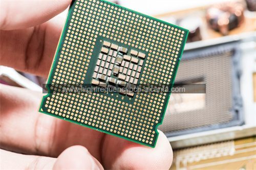
Minimum Gap PCB Manufacturer
Minimum Gap PCB Manufacturer,Minimum Gap PCBs are designed with extremely tight spacing between circuit traces and components to maximize board real estate and accommodate high-density designs. These PCBs are engineered to ensure reliable electrical performance despite the reduced spacing, which requires precise manufacturing and stringent quality control. The minimized gaps help to achieve compact and efficient designs, making them suitable for applications such as smartphones, tablets, and other space-constrained electronic devices. By reducing the gap between elements, Minimum Gap PCBs enable higher functionality within a smaller footprint, while maintaining signal integrity and electrical reliability in high-performance electronic systems.
What is Minimum Gap PCB?
Minimum Gap PCB, also known as Minimum Clearance PCB, refers to a type of printed circuit board designed with extremely narrow spacing between its conductive elements, such as traces, pads, and vias. This design approach is essential in high-density applications where space is limited, and maximizing the board’s functionality and layout efficiency is crucial.
In Minimum Gap PCBs, the distance between these elements is reduced to the absolute minimum required to maintain electrical isolation and prevent short circuits. This design must adhere to strict manufacturing tolerances and standards to ensure reliability and performance. Key factors influencing the design of Minimum Gap PCBs include the type of dielectric material used, the thickness of the copper layers, and the precision of the PCB manufacturing process.
The benefits of Minimum Gap PCBs are particularly significant in advanced electronics where compact designs are essential, such as in smartphones, tablets, and other high-performance devices. By reducing the spacing between components, designers can fit more functionality into a smaller footprint, which can lead to improved performance and reduced overall size of the electronic device.
However, designing and manufacturing Minimum Gap PCBs presents challenges, including increased complexity in the fabrication process and potential issues with signal integrity and heat dissipation. To address these challenges, manufacturers must employ advanced technologies and materials, as well as rigorous quality control measures, to ensure that the final product meets the required performance and reliability standards.
Minimum Gap PCB Manufacturer
What are the Minimum Gap PCB Design Guidelines?
Designing Minimum Gap PCBs requires careful consideration to ensure reliable performance and manufacturability. Here are some key guidelines to follow:
- Clearance Specifications: Adhere to the minimum clearance requirements specified by the PCB manufacturer and industry standards. These guidelines will vary depending on factors like voltage levels and signal frequencies.
- Signal Integrity: Pay attention to signal integrity, especially for high-speed signals. Minimizing gaps can affect impedance and cause crosstalk. Use controlled impedance traces and differential pairs if necessary to maintain signal quality.
- Thermal Management: With smaller gaps, heat dissipation becomes a critical issue. Ensure adequate thermal management solutions are in place, such as heat sinks or thermal vias, to prevent overheating of components.
- Design for Manufacturability: Verify that the design is manufacturable with the chosen PCB fabricator’s capabilities. Work closely with your PCB manufacturer to understand their minimum gap requirements and production tolerances.
- Component Placement: Optimize component placement to minimize trace lengths and avoid routing between closely spaced components. Ensure that components are placed with sufficient space for soldering and maintenance.
- Testing and Inspection: Implement thorough testing and inspection procedures to detect any potential issues related to minimum gaps. Automated optical inspection (AOI) and other testing methods can help ensure quality and reliability.
- Material Selection: Choose high-quality PCB materials that can withstand the tight tolerances required for minimum gap designs. Consider factors such as dielectric strength, thermal stability, and mechanical properties.
- Electrical Considerations: For high-frequency or high-current applications, ensure that the reduced gaps do not lead to electrical issues like unintended coupling or signal degradation.
- Design Software: Use advanced PCB design software that supports minimum gap design rules and can accurately simulate the effects of tight spacing on electrical performance.
- Compliance and Standards: Follow relevant industry standards and guidelines, such as IPC-2221 or IPC-7351, to ensure that the design meets accepted quality and safety criteria.
By adhering to these guidelines, you can effectively manage the challenges associated with Minimum Gap PCB designs and achieve a reliable and high-performance circuit board.
What is the Minimum Gap PCB Fabrication Process?
The fabrication process for Minimum Gap PCBs involves several critical steps to ensure that the PCB meets stringent design requirements and performs reliably. Here’s a breakdown of the typical process:
- Design and Layout: The process begins with the design and layout of the PCB, where the minimum gap requirements are defined. Advanced PCB design software is used to create detailed schematics and layouts, ensuring that the design adheres to the specified clearance and spacing constraints.
- Photomask Creation: Once the design is finalized, photomasks are created. These masks are used to transfer the PCB design onto the copper layers of the board. For Minimum Gap PCBs, the precision of the photomask is crucial to achieve the tight tolerances required.
- Copper Layer Deposition: A thin layer of copper is deposited onto the PCB substrate, typically through a process called electroplating. This copper layer will form the conductive traces, pads, and vias.
- Photoresist Application: A photoresist layer is applied to the copper-clad substrate. This light-sensitive material will protect certain areas of the copper during the etching process. For minimum gap designs, the photoresist layer must be precisely applied to ensure accurate pattern transfer.
- Exposure and Development:The photoresist-coated board is exposed to UV light through the photomask. The areas exposed to light become hard and resistant to etching, while the unexposed areas remain soft. The board is then developed to remove the soft photoresist, revealing the copper pattern underneath.
- Etching: The board is subjected to an etching process to remove the unwanted copper, leaving behind the desired trace patterns. In minimum gap PCBs, precise etching is essential to ensure that the narrow spaces between traces are accurately maintained.
- Drilling and Plating: Holes for vias and component leads are drilled into the PCB. These holes are then plated with a thin layer of copper to provide electrical connections between different layers of the PCB.
- Solder Mask Application: A solder mask is applied over the PCB to protect the copper traces and prevent solder from bridging between components during assembly. For minimum gap designs, the solder mask must be precisely aligned to avoid issues with soldering and short circuits.
- Surface Finish: The PCB undergoes a surface finishing process, such as HASL (Hot Air Solder Leveling), ENIG (Electroless Nickel/Immersion Gold), or other methods, to provide a solderable surface and protect the copper traces.
- Inspection and Testing:The fabricated PCB is inspected and tested for quality and performance. This includes visual inspection, automated optical inspection (AOI), and electrical testing to ensure that the minimum gap specifications are met and that the board functions correctly.
- Final Assembly: After passing inspection, the PCB is prepared for final assembly. This may include adding components, soldering, and performing additional testing to ensure that the final product meets all performance and reliability requirements.
By carefully managing each step of this process, manufacturers can successfully produce Minimum Gap PCBs that meet the tight design constraints and deliver high performance in their intended applications.
How Do You Manufacture Minimum Gap PCB?
Manufacturing Minimum Gap PCBs requires precision and careful control throughout the production process. Here’s an overview of the steps involved in manufacturing Minimum Gap PCBs:
- Design Preparation: Begin with a detailed PCB design that specifies minimum gaps between traces, pads, and vias. Utilize advanced PCB design software to ensure that all design rules and spacing constraints are accurately defined.
- Fabrication File Generation: Generate fabrication files, including Gerber files, which provide the detailed layout information needed for manufacturing. These files are used to create photomasks and guide the fabrication process.
- Photomask Production: Create high-precision photomasks based on the design files. These masks are essential for transferring the PCB design onto the copper layers and must be manufactured with extreme accuracy to maintain the tight gap specifications.
- Copper Layer Deposition: Deposit a thin layer of copper onto the PCB substrate using processes such as sputtering or electroplating. This copper layer will form the conductive traces, pads, and vias.
- Photoresist Coating: Apply a photoresist layer to the copper-clad board. This light-sensitive material will protect specific areas of the copper during etching. Ensure that the photoresist is uniformly applied to avoid issues with pattern fidelity.
- Exposure and Development: Expose the photoresist-coated board to UV light through the photomasks. This process hardens the photoresist in the exposed areas. Develop the board to remove the unexposed photoresist, revealing the copper pattern beneath.
- Etching: Perform the etching process to remove the excess copper and leave the desired trace patterns. For minimum gap designs, precise etching is crucial to achieve the narrow spacing between traces and avoid short circuits.
- Drilling and Plating: Drill holes for vias and component leads. Plate these holes with copper to create electrical connections between different layers of the PCB. Ensure that the drilling and plating processes are accurate to maintain the integrity of the minimum gap design.
- Solder Mask Application: Apply a solder mask to protect the copper traces and prevent solder bridging during assembly. For minimum gap designs, precise alignment of the solder mask is essential to avoid soldering issues.
- Surface Finish:Apply a surface finish, such as HASL, ENIG, or another method, to protect the copper traces and provide a solderable surface. Choose a finish that meets the requirements of the specific application and maintains the tight gap specifications.
- Inspection and Testing: Conduct thorough inspection and testing to ensure that the PCB meets all design specifications and quality standards. This includes visual inspection, automated optical inspection (AOI), and electrical testing to verify that the minimum gaps are correctly maintained.
- Final Assembly: Prepare the PCB for final assembly, which may involve adding components, soldering, and performing additional testing to ensure that the completed PCB functions as intended.
By meticulously controlling each step of the manufacturing process and utilizing advanced technologies, manufacturers can produce Minimum Gap PCBs that meet the stringent design requirements and deliver high performance in their intended applications.
How Much Should Minimum Gap PCB Cost?
The cost of Minimum Gap PCBs can vary widely based on several factors, including design complexity, manufacturing specifications, and quantity. Here’s an overview of the factors influencing the cost and a general idea of what to expect:
- Design Complexity: The complexity of the PCB design, including the number of layers, the tightness of the gaps, and the presence of high-density features, significantly impacts the cost. More complex designs require advanced manufacturing techniques and higher precision, which can increase costs.
- Gap Size: The smaller the minimum gap, the more challenging and precise the manufacturing process becomes. Tight gaps require advanced photomask and etching technologies, which can raise production costs.
- Quantity: The volume of PCBs ordered affects the per-unit cost. Generally, higher quantities lead to lower per-unit costs due to economies of scale. However, initial setup costs for low-volume production can be higher.
- Material Selection: The choice of PCB substrate materials, such as high-frequency laminates or specialized dielectrics, can impact the cost. Premium materials used for high-performance applications typically come with higher costs.
- Layer Count: The number of layers in the PCB affects the cost. Multilayer PCBs with minimum gaps require more complex manufacturing processes and materials, increasing the overall cost.
- Surface Finish: The type of surface finish applied to the PCB also influences the cost. Finishes like ENIG or other high-end options can be more expensive than basic HASL finishes.
- Manufacturing Technology: Advanced manufacturing technologies, such as laser drilling, fine-line etching, and high-precision photomasks, contribute to higher costs. The use of these technologies is often necessary for minimum gap designs.
- Testing and Quality Control: Rigorous testing and quality control processes ensure that the PCBs meet design specifications and performance standards. Comprehensive testing can add to the overall cost.
Ultimately, the exact cost of Minimum Gap PCBs will depend on your specific design and manufacturing requirements. It’s advisable to request quotes from multiple PCB manufacturers to get a detailed cost estimate based on your project’s needs.
What is Minimum Gap PCB Base Material?
The base material of a Minimum Gap PCB plays a crucial role in determining the board’s performance, reliability, and manufacturability. Here’s an overview of the key base materials used for Minimum Gap PCBs:
- FR-4: The most common PCB base material, FR-4 is a composite of woven glass fabric and epoxy resin. It offers good mechanical properties, electrical insulation, and is cost-effective. However, for extremely tight gaps and high-frequency applications, other materials may be preferred due to FR-4’s limitations in high-speed performance.
- High-Frequency Laminates: For PCBs designed to handle high-frequency signals, materials like Rogers or Taconic laminates are used. These materials have low dielectric loss and stable electrical properties, which are crucial for maintaining signal integrity in high-frequency applications. They can support tighter gaps without compromising performance.
- Polyimide:Polyimide-based materials are known for their excellent thermal stability and flexibility. They are used in applications requiring high thermal resistance and can accommodate tighter spacing and high-density designs without deformation.
- Ceramic Substrates: For advanced applications, especially those requiring high thermal conductivity and electrical performance, ceramic substrates (such as aluminum nitride or beryllium oxide) are used. These materials provide superior thermal management and are suitable for high-performance Minimum Gap PCBs.
- Metal Core PCBs: Metal core materials, like aluminum or copper, are used in applications requiring efficient heat dissipation. These substrates are typically employed in LED lighting or high-power electronic applications, and can be designed with minimum gaps to handle high thermal loads effectively.
- PTFE (Polytetrafluoroethylene): PTFE is used for very high-frequency applications due to its low dielectric constant and loss tangent. It’s often used in RF (radio frequency) and microwave PCBs, where maintaining precise gaps is crucial for signal integrity.
Choosing the right base material is essential for ensuring that a Minimum Gap PCB meets its design specifications and performs reliably in its intended application.
Which Company Makes Minimum Gap PCB?
There are many companies in the market that manufacture Minimum Gap PCBs, each catering to different needs. For example, companies such as Shenghua Technology from Taiwan, Cypress Semiconductor from the USA, Yaskawa Electric Corporation from Japan, Bettis from Germany, and Hongbo Electronics from China all offer high-performance PCBs that meet stringent gap requirements. These companies have advanced technology and equipment, and their products are widely used in consumer electronics, automotive electronics, communication devices, and other fields.
Shenghua Technology is renowned for its excellent High-Density Interconnect (HDI) technology, providing reliable solutions for designs with minimum gaps. Cypress Semiconductor has extensive experience in PCB design and manufacturing, with products used in various electronic devices. Yaskawa Electric specializes in precision electronics manufacturing, producing high-precision Minimum Gap PCBs. Bettis has accumulated rich experience in high-end PCB manufacturing, offering high-quality Minimum Gap PCB products. Hongbo Electronics has a broad influence in the Chinese market, with products that perform exceptionally well in minimum gap designs.
Our company also has the capability to manufacture Minimum Gap PCBs. Our products use high-performance substrate materials and advanced manufacturing technology to ensure excellent performance even under strict gap requirements. The features of our Minimum Gap PCB products include:
- High Precision Processing: We have advanced production equipment and technical teams capable of achieving high-precision trace processing and lamination, ensuring that the product meets minimum gap requirements.
- Quality Substrate Materials: We use high-quality substrate materials such as high-frequency materials and high-performance resins to ensure stability and reliability in high-density applications.
- Multilayer Structure Design: We can design and manufacture multilayer Minimum Gap PCBs according to customer needs, meeting the requirements of complex circuits.
- Comprehensive Quality Control: We implement strict quality control measures at every stage, from design and manufacturing to testing, ensuring high-quality products.
- Customized Services: We offer customized PCB design and manufacturing services, adjusting and optimizing based on specific customer requirements to ensure the product fully meets application needs.
Through continuous technological innovation and rigorous quality management, our Minimum Gap PCB products are widely recognized in the market and are used in various high-density electronic devices. If you have a need for Minimum Gap PCBs, please contact us, and we will be dedicated to providing you with high-quality products and services.
In summary, whether it is material selection, processing technology, or after-sales service, our company is capable of producing high-quality Minimum Gap PCBs that meet the needs of various high-density applications.
What are the 7 Qualities of Good Customer Service?
Good customer service is critical for building customer satisfaction and loyalty. Here are seven key qualities that define excellent customer service:
- Responsiveness:Timely and efficient responses to customer inquiries and issues are crucial. Good customer service ensures that customers receive prompt attention and that their concerns are addressed quickly, reducing wait times and improving satisfaction.
- Empathy: Understanding and acknowledging the customer’s feelings and perspectives is essential. Empathetic service involves listening actively, showing genuine concern, and making customers feel valued and understood.
- Knowledge: Customer service representatives should have a deep understanding of the products or services they are supporting. They need to provide accurate information, resolve issues effectively, and offer informed recommendations.
- Communication Skills: Clear, concise, and courteous communication is key. Good customer service involves using appropriate language, avoiding jargon, and ensuring that the customer fully understands the information and solutions provided.
- Patience:Handling customers with patience, especially those who are frustrated or confused, is important. Patience helps in addressing concerns calmly and ensures that the customer feels supported throughout the interaction.
- Problem-Solving Ability:Effective customer service involves diagnosing issues, providing solutions, and making necessary adjustments to meet the customer’s needs. Strong problem-solving skills enable representatives to address and resolve problems efficiently.
- Follow-Up: Ensuring that issues are resolved to the customer’s satisfaction and following up to confirm that solutions were effective demonstrates commitment to customer satisfaction. Good customer service involves checking back to make sure customers are happy with the outcome.
By embodying these qualities, businesses can create a positive customer experience, foster long-term relationships, and build a strong reputation for excellent service.
FAQs about Minimum Gap PCB
What is a Minimum Gap PCB?
A Minimum Gap PCB (Printed Circuit Board) is a type of PCB where the spacing between conductive traces, pads, and vias is minimized. This design is used to achieve higher density and compactness in electronic circuits.
Why are Minimum Gap PCBs used?
Minimum Gap PCBs are used to accommodate more components in a smaller area, which is crucial for compact and high-density electronic devices. They help in reducing the overall size of the PCB and improving performance in high-speed and high-frequency applications.
What are the key challenges in manufacturing Minimum Gap PCBs?
Manufacturing Minimum Gap PCBs involves challenges such as achieving precise etching, maintaining accurate spacing, and ensuring reliable electrical performance. The process requires advanced technology and careful quality control to avoid issues like short circuits and signal interference.
What materials are commonly used for Minimum Gap PCBs?
Common materials include high-frequency laminates (like Rogers or Taconic), polyimide, FR-4, and metal core substrates. The choice depends on the specific application requirements, such as thermal management and electrical performance.
How does the gap size affect PCB performance?
Smaller gaps can lead to improved signal density and more compact designs. However, they also require more precise manufacturing processes to avoid problems like electrical interference or signal degradation.
What industries commonly use Minimum Gap PCBs?
Minimum Gap PCBs are commonly used in industries such as telecommunications, consumer electronics, automotive, and aerospace. They are ideal for applications that require high-density circuitry and compact form factors.