 Professional high frequency circuit board supplier

Minimum Clearance PCB Manufacturer
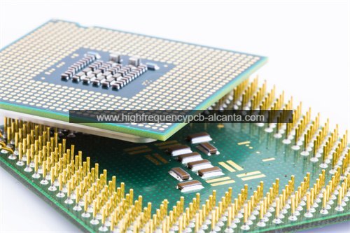
Minimum Clearance PCB Manufacturer,Minimum Clearance PCBs refer to printed circuit boards designed with minimal spacing between conductive traces and components. These boards are crucial for high-density electronic designs where efficient use of space is essential. By minimizing clearance distances, Minimum Clearance PCBs reduce signal interference and electromagnetic interference (EMI), enhancing overall electrical performance and reliability. They are widely used in applications requiring compact layouts and precise signal routing, such as mobile devices, IoT gadgets, and aerospace equipment. Manufacturing these PCBs requires precision to ensure compliance with stringent design guidelines and standards, ensuring optimal functionality and durability in modern electronic devices.
What is a Minimum Clearance PCB?
A Minimum Clearance PCB refers to the design and manufacturing requirement for the minimum distance between components, traces, and other electrical elements on a printed circuit board (PCB). This design is often used in high-density integrated circuits (HDI) and compact electronic devices to provide more functionality and connectivity within limited space.
In a Minimum Clearance PCB, manufacturers must adhere to specific spacing standards to ensure the normal operation and reliability of the circuit. Too small a spacing can lead to electrical short circuits, signal interference, or other performance issues. Therefore, designers need to consider these parameters early in the design phase and optimize space usage during layout.
To achieve minimum clearance design, PCB manufacturers often utilize advanced processing technologies, such as laser etching and micro-manufacturing, to ensure high precision and quality. Additionally, using high-frequency materials and special insulating materials helps improve performance and reduce signal loss.
In terms of applications, Minimum Clearance PCBs are widely used in mobile devices, consumer electronics, medical devices, and automotive electronics. With the continuous advancement of technology, their design and manufacturing techniques are also progressing, supporting smaller and higher-performance electronic products. In summary, Minimum Clearance PCBs represent an important engineering technology that drives innovation and development in the electronics industry.
Minimum Clearance PCB Manufacturer
What are the Minimum Clearance PCB Design Guidelines?
Here are some key Minimum Clearance PCB Design Guidelines:
- Follow IPC Standards: Adhere to IPC standards, such as IPC-2221 and IPC-2222, which provide general design and clearance requirements.
- Component Spacing: Ensure adequate spacing between components to prevent mechanical interference and facilitate assembly.
- Trace Clearance: Maintain minimum trace-to-trace spacing, considering factors like voltage levels, frequency, and the PCB material. High-voltage areas should have larger clearances.
- Via Clearance: Ensure that vias have sufficient clearance from traces and pads to avoid unintentional connections.
- Ground Plane Considerations: Keep a minimum distance between signal traces and ground planes to reduce noise and improve signal integrity.
- Thermal Management: Design with thermal relief in mind, ensuring that heat-generating components have adequate space and thermal vias for heat dissipation.
- Manufacturing Capabilities: Consult with PCB manufacturers to understand their specific capabilities regarding minimum clearances, as this can vary by technology and equipment.
- Simulation Tools: Use simulation tools to analyze signal integrity and electromagnetic interference (EMI) impacts due to reduced spacing.
- Design Rule Checks (DRC): Utilize DRC features in PCB design software to automate clearance checks and ensure compliance with defined guidelines.
- Prototype Testing: After designing, prototype and test to validate performance, especially under conditions that may affect clearance requirements.
By following these guidelines, designers can optimize the performance and reliability of Minimum Clearance PCBs.
What is the Minimum Clearance PCB Fabrication Process?
The Minimum Clearance PCB fabrication process involves several key steps to ensure precision and reliability. Here’s an overview:
- Design and Layout: Utilize PCB design software to create a layout that adheres to minimum clearance requirements. Implement design rule checks (DRC) to verify spacing between traces, components, and vias.
- Photolithography:Print the PCB design onto a photomask. The mask allows selective exposure of the substrate, forming the circuit pattern.
- Substrate Preparation:Prepare the PCB substrate, typically made from materials like FR-4 or Rogers. Clean the surface to remove contaminants that could affect adhesion.
- Coating:Apply a photosensitive resist to the substrate. This resist will protect parts of the board during etching.
- Exposure:Expose the coated substrate to UV light through the photomask. The exposed areas of the resist become soluble, allowing for the next steps.
- Development:Develop the exposed substrate to wash away the soluble resist, revealing the copper areas where traces will be formed.
- Etching:Use an etching solution to remove unwanted copper, leaving only the desired circuit traces defined by the remaining resist.
- De-resist and Cleaning:Remove the remaining resist layer and clean the PCB to ensure a smooth surface for subsequent processes.
- Drilling:Drill holes for vias and mounting components. Precision drilling is crucial to maintain minimum clearance standards.
- Plating:Apply a conductive layer in drilled vias, often through electroplating, to establish electrical connections.
- Final Finishing:Apply surface finishes (such as HASL or ENIG) to improve solderability and protect the copper traces.
- Inspection and Testing:Conduct visual inspections and electrical testing to ensure that all clearances are maintained and that the board meets design specifications.
- Cutting and Routing:Cut the PCBs to their final size and shape, ensuring that edges do not interfere with any component placement.
By following this meticulous fabrication process, manufacturers can produce Minimum Clearance PCBs that meet performance and reliability standards.
How do you manufacture a Minimum Clearance PCB?
Manufacturing a Minimum Clearance PCB involves several precise steps to ensure the required spacing and overall quality. Here’s a streamlined overview of the process:
- Design and Planning:Use PCB design software to create the layout, ensuring compliance with minimum clearance requirements. Perform design rule checks (DRC) to validate spacing between components, traces, and vias.
- Create Photomasks:Generate photomasks based on the design. These masks will guide the exposure of the PCB substrate during the photolithography process.
- Substrate Preparation:Clean and prepare the substrate material, typically FR-4 or another suitable dielectric material, to ensure a contaminant-free surface.
- Apply Photoresist:Coat the cleaned substrate with a photosensitive resist. This layer will protect areas of copper during etching.
- Exposure:Expose the coated substrate to ultraviolet (UV) light through the photomask. This process hardens the resist in the desired patterns, defining where copper will remain.
- Development:Develop the exposed substrate by washing away the unexposed resist, revealing the copper areas for etching.
- Etching:Use chemical etching to remove the unwanted copper, leaving behind the desired circuit traces as defined by the remaining photoresist.
- Remove Photoresist:Strip away the remaining photoresist, resulting in a clean copper pattern on the substrate.
- Drilling:Drill precision holes for vias and component leads, ensuring that they meet the specified minimum clearances.
- Plating:Electroplate the drilled vias with a conductive layer to establish electrical connections. This step also enhances the robustness of the vias.
- Surface Finish:Apply surface finishes (e.g., HASL, ENIG) to the copper traces to protect them and improve solderability.
- Inspection and Testing:Conduct visual inspections and electrical testing to ensure that the PCB meets design specifications and that minimum clearances are maintained.
- Cutting and Routing:Cut and route the PCBs to their final size, ensuring that edges do not compromise any components or connections.
By following these detailed steps, manufacturers can effectively produce Minimum Clearance PCBs that meet the demands of high-density applications.
How much should a Minimum Clearance PCB cost?
The cost of a Minimum Clearance PCB can vary widely based on several factors, including:
- Complexity of Design: More complex designs with intricate layouts, multiple layers, or specialized components will generally cost more.
- Material Type: The choice of substrate material (e.g., FR-4, Rogers) and surface finish (e.g., HASL, ENIG) can impact costs.
- Quantity: Larger production runs typically reduce the per-unit cost due to economies of scale.
- Manufacturing Process: Advanced manufacturing techniques, such as HDI (High-Density Interconnect), may increase costs due to the additional precision required.
- Turnaround Time: Rush orders or expedited manufacturing processes can lead to higher prices.
- Additional Features: Extra features like vias, impedance control, or special treatments can also affect the overall cost.
Generally, for a basic Minimum Clearance PCB, prices might range from $1 to $10 per square inch for small quantities. For larger quantities or more complex designs, prices can be lower per unit. It’s advisable to obtain quotes from multiple manufacturers to get a precise estimate based on specific design requirements.
What is Minimum Clearance PCB base material?
Minimum Clearance PCB base material refers to the substrate used in the construction of printed circuit boards that require specific spacing between traces, components, and vias. Common base materials include:
- FR-4: A widely used fiberglass-reinforced epoxy laminate, known for its good electrical insulation and mechanical properties.
- Rogers Materials: Such as Rogers 4350B or 5880, which are designed for high-frequency applications, offering better dielectric properties and thermal management.
- High-TG Epoxy: These materials have a higher glass transition temperature, suitable for applications requiring thermal stability.
- Ceramic Substrates: Used in high-frequency or high-power applications, providing excellent thermal conductivity and dielectric properties.
- Polyimide: Known for high thermal stability and flexibility, often used in applications with strict space constraints.
Selecting the appropriate base material is crucial for ensuring performance, reliability, and manufacturability of Minimum Clearance PCBs, particularly in high-density and high-frequency applications.
Which company makes Minimum Clearance PCBs?
There are many companies that manufacture Minimum Clearance PCBs, including both large international electronics manufacturers and specialized PCB producers. Notable international companies such as Mouser Electronics and Digi-Key Electronics, as well as domestic companies like Dazhong Laser and Ruikeda Electronics in China, offer a variety of PCB specifications, including those suitable for high-density and high-frequency applications.
In China, specialized PCB manufacturers such as Shenzhen Chuanglianzhong Electronics Co., Ltd., Guangdong Xingguang Circuit Technology Co., Ltd., and Jiangsu Zhengfeng Electronics Technology Co., Ltd. have the capability to produce Minimum Clearance PCBs. These companies typically possess advanced production equipment and technical teams capable of customizing and producing PCBs that meet specific standards based on customer requirements.
Our company is also a professional PCB manufacturer with years of industry experience and technological expertise. We can provide various types of PCB products, including high-density Minimum Clearance PCBs. Our manufacturing capabilities cover everything from PCB design and prototyping to mass production, allowing us to flexibly meet different customer needs.
Specifically, our manufacturing capabilities include:
- Advanced Manufacturing Equipment: We have invested in state-of-the-art PCB manufacturing equipment, including high-precision laser etching machines, automated production lines, and precise inspection equipment, ensuring the production of high-quality PCB products.
- Strict Quality Control: We implement rigorous quality control processes, ensuring that every step from raw material procurement to the production process is tightly monitored, guaranteeing that products meet customer design requirements and industry standards.
- Customized Services: We offer tailored PCB solutions based on specific design requirements and application scenarios. Whether it’s a complex layer structure, high-frequency requirements, or Minimum Clearance designs, we can meet customer demands.
- Fast Delivery: With efficient production capabilities and flexible scheduling, we can promptly respond to customer orders and ensure delivery within the specified timeframe.
Through our professional manufacturing capabilities and excellent service, we are committed to providing high-quality Minimum Clearance PCB products to support our customers’ innovation and development in the electronics industry.
What are the 7 qualities of good customer service?
Here are seven qualities of good customer service:
- Empathy:Understanding and sharing the feelings of customers, which helps build a connection and shows that their concerns are valued.
- Responsiveness: Timely responses to inquiries or issues, demonstrating that the company prioritizes customer needs and is eager to help.
- Knowledge: Having a deep understanding of products, services, and policies, enabling staff to provide accurate information and effective solutions.
- Patience: Remaining calm and patient, especially when dealing with frustrated or confused customers, ensuring a positive interaction.
- Clear Communication: Conveying information clearly and effectively, using simple language to avoid misunderstandings and enhance customer understanding.
- Problem-Solving Skills: Ability to think critically and find solutions to customer issues, showing resourcefulness and commitment to customer satisfaction.
- Positive Attitude: Maintaining a friendly and upbeat demeanor, which creates a welcoming atmosphere and enhances the overall customer experience.
These qualities contribute to building strong customer relationships and fostering loyalty.
FAQs
Why is minimum clearance important?
Maintaining minimum clearance helps prevent electrical shorts, signal interference, and ensures reliable operation, especially in compact designs.
What materials are used for Minimum Clearance PCBs?
Common materials include FR-4, Rogers substrates, high-TG epoxy, and polyimide, chosen based on application requirements.
What factors affect the cost of Minimum Clearance PCBs?
Costs can vary based on design complexity, material choice, manufacturing processes, quantity, and turnaround time.
How can I ensure my design meets minimum clearance requirements?
Utilize PCB design software with DRC (Design Rule Check) features, consult IPC standards, and work closely with your PCB manufacturer for specifications.
Can Minimum Clearance PCBs be produced in large quantities?
Yes, many manufacturers can produce Minimum Clearance PCBs in both small and large quantities, benefiting from economies of scale.
What industries commonly use Minimum Clearance PCBs?
They are widely used in consumer electronics, telecommunications, automotive, medical devices, and aerospace due to their compactness and efficiency.
Are there any design tools to assist with Minimum Clearance PCB layouts?
Yes, many PCB design software packages offer tools specifically for managing clearances, including automated DRC and layout optimization features.