 Professional high frequency circuit board supplier
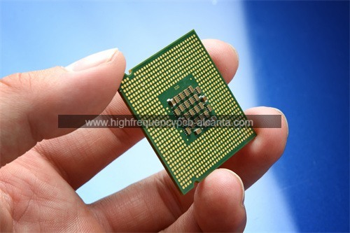
What is High speed PCB?
High speed PCB Manufacturer,High-speed PCBs are specialized circuit boards designed to efficiently transmit data at rapid rates. Engineered with materials like high-frequency laminates and controlled impedance traces, they minimize signal degradation and ensure reliable performance in demanding applications. High-speed PCBs feature precise routing, impedance matching, and signal integrity techniques, enabling seamless data transmission in telecommunications, computing, and automotive systems. These PCBs undergo rigorous testing and adhere to stringent design guidelines to meet industry standards for high-speed data transmission. With their advanced construction and meticulous design, high-speed PCBs facilitate the development of cutting-edge electronic devices with superior performance and reliability.
A High-Speed PCB, commonly known as a Printed Circuit Board, is specifically engineered to adeptly manage the rapid transmission of signals and operate seamlessly at high frequencies. Its significance is paramount in applications like telecommunications, networking, computers, and advanced electronic devices, where precise timing and unwavering signal integrity are non-negotiable.
The design intricacies of high-speed PCBs demand a meticulous approach to curbing signal distortion, mastering impedance, and thwarting electromagnetic interference (EMI) and radio frequency interference (RFI). These considerations are pivotal, ensuring that transmitted data completes its journey without succumbing to undesirable distortion or noise.
The construction of high-speed PCBs often involves the utilization of advanced materials with tailored dielectric properties to meet the demands of high-frequency signals. Designers employ a strategic dance of exacting routing techniques, controlled impedance traces, and thoughtful component placement to mitigate potential pitfalls like signal reflections and crosstalk.
A heightened focus is directed toward optimizing the ground and power distribution systems of high-speed PCBs. This meticulous attention ensures a steadfast power supply and diminishes the impact of noise on delicate signals. Simulation tools are commonly enlisted in the design process, enabling a thorough analysis and refinement of the PCB layout before it embarks on the journey of actual manufacturing, thereby guaranteeing compliance with stringent performance requirements.
In essence, a high-speed PCB stands as an eloquently engineered circuit board, facilitating the swift propagation of signals, minimizing degradation, and upholding signal integrity in the intricate dance of electronic systems operating at elevated frequencies.
High speed PCB Manufacturer
What are the functions of High speed PCB?
At the heart of electronic systems requiring rapid and precise signal handling, high-speed PCBs stand as indispensable linchpins. Their multifaceted functionality is geared towards meeting the exacting demands of applications where impeccable timing, unwavering reliability, and pristine signal integrity are indispensable.
Signal Dynamics: Operating as the backbone of signal transmission, high-speed PCBs excel in ensuring the swift and accurate conveyance of data. Through meticulous design nuances, these boards mitigate signal degradation, ensuring the seamless flow of information.
Timing Finesse and Syncopation: In realms such as high-performance computing and communication systems, high-speed PCBs contribute to the orchestration of impeccable timing. Their role extends to synchronizing signals with finesse, ensuring a harmonious and synchronized dance within the system.
Impedance Choreography: Mastery over controlled impedance is a defining feature of high-speed PCBs, especially crucial for the nuanced handling of high-frequency signals. Employing sophisticated trace geometries and materials, these boards choreograph impedance matching to perfection, averting distortions and reflections.
Crosstalk Minuet: The intricate dance of signals within high-speed PCBs is meticulously choreographed to evade the disruptive interference known as crosstalk. Thoughtful design elements, including precise trace spacing and shielding, ensure a graceful minuet where signals remain distinct.
EMI/RFI Harmonics: Inherent to high-speed signals is the generation of electromagnetic interference (EMI) and radio frequency interference (RFI). High-speed PCBs harmonize with these challenges through robust grounding, shielding mechanisms, and effective filtering, ensuring a symphony free from disruptive interferences.
Power Distribution Symphony: Orchestrating the symphony of power distribution, high-speed PCBs minimize power losses, conduct stable power delivery, and attenuate the impact of power-induced noise on sensitive signals. This ensures a harmonious power distribution across the system.
Heat Dissipation Ballet: Given the thermal dynamics involved in rapid signal transmission, high-speed PCBs engage in a ballet of heat dissipation. Introducing elements like heat sinks, strategically placed vias, and specific materials, these boards choreograph the dissipation of heat with grace and efficiency.
Advanced Component Integration Sonata: In the ever-evolving cadence of technology, high-speed PCBs seamlessly integrate with sophisticated electronic components such as high-speed processors and memory modules. Their design harmonizes with the specific requirements of these components, resulting in a symphonic integration that delivers optimal performance.
In essence, high-speed PCBs are virtuosos in the realm of electronic systems, directing a symphony of functions that ensure impeccable signal transmission, timing precision, and reliability in applications that demand the utmost finesse and integrity.
What are the different types of High speed PCBs?
The world of high-speed PCBs unfolds with a rich tapestry of types, each finely tuned to its unique set of performance demands and application intricacies. These variations exemplify the adaptability and precision required in the art of circuit board design.
Digital Velocity PCBs: Engineered to navigate the swift currents of data processing and transmission, these boards find their home in the intricate landscapes of microprocessors, memory modules, and digital communication systems.
RF (Radio Frequency) Envoys: Tailored to waltz within the radio frequency spectrum, these boards take center stage in the wireless ballet of communication devices, radar systems, and RF transceivers. Their choreography allows for the nimble handling of high-frequency signals.
Mixed-Signal Harmonizers: Conducting the symphony of both analog and digital signals, these boards seamlessly blend the notes of data converters, sensor interfaces, and communication systems where the orchestra of analog and digital components plays in harmony.
Power Distribution Virtuosos: Taking up the baton in high-performance computing and server applications, these boards conduct the power symphony. They distribute power with finesse, minimizing losses and preserving the integrity of the signal melody.
Backplane Maestros: Leading the ensemble in systems with multiple interconnected modules, these boards facilitate a high-speed communication sonata between distinct subsystems or modules, akin to a musical backplane.
Flex Melodies (Flexible Printed Circuit Boards): With the grace of dancers, these boards adapt to non-planar surfaces, finding a stage in applications with unconventional form factors, where flexibility is key.
HDI (High-Density Interconnect) Composers: Crafting intricate patterns of wiring density, multiple layers, and fine-pitch components, HDI PCBs are the virtuosos of compact electronic devices like smartphones, where space is a premium.
EMI/RFI Safeguards: Donning the armor of shields, these boards minimize the interference dissonance. They ensure that the electromagnetic and radio frequency interferences are kept at bay, preserving the harmony of sensitive signals.
High-Frequency Analog Virtuosos: Conducting with precision in analog signal landscapes, these boards find resonance in audio equipment, medical devices, and scientific instruments where the accuracy of notes is paramount.
DDR (Double Data Rate) Orchestras: Directed toward the demands of high-speed memory interfaces like DDR3, DDR4, or DDR5, these boards lead the orchestration of efficient communication between processors and memory modules in computing systems.
This kaleidoscope of high-speed PCB types paints a vivid picture of the intricate dance between design nuances and application requirements, underscoring the need for bespoke solutions in the dynamic world of electronic design.
What are the main structures and production technologies of High speed PCB?
High-speed PCBs feature distinctive structures and employ advanced production technologies to meet the demanding requirements of rapid signal transmission and signal integrity maintenance. The key components and production techniques include:
Layered Complexity: High-speed PCBs often adopt a multi-layered structure, enabling intricate signal routing. The layer stack-up is meticulously designed to control impedance, minimize crosstalk, and efficiently manage power distribution.
Controlled Impedance Mastery: The traces carrying high-frequency signals are crafted with controlled impedance, a critical aspect to prevent signal distortions and reflections. This involves precise adjustments in trace width, spacing, and the use of specific dielectric materials.
Ground and Power Precision: Ground planes, when expertly crafted, serve as linchpins in the quest to mitigate electromagnetic interference (EMI) and furnish a steadfast reference for signals. Power planes are structured for efficient distribution, mitigating noise and ensuring signal integrity.
Via Innovation: Vias are indispensable for connecting different PCB layers. High-speed designs often incorporate blind and buried vias, facilitating intricate layouts while preserving signal integrity.
Surface Finish Excellence: Surface finishes impact reliability and performance. ENIG (Electroless Nickel Immersion Gold) and immersion silver are preferred in high-speed applications for their flat surfaces and superior solderability.
Dielectric Material Selection: The dielectric material between layers is carefully chosen to control signal propagation. Advanced materials with specific dielectric constants are often employed to support the demands of high-frequency signals.
Precision Routings and Serpentine Traces: Careful routing minimizes signal skew and ensures signal integrity. Serpentine traces are utilized to equalize the lengths of parallel traces, reducing timing discrepancies.
Differential Pair Expertise: In high-speed designs, the adoption of differential signaling is a prevalent strategy aimed at diminishing electromagnetic interference. Meticulous routing of differential pairs involves stringent control over impedance and exact spacing, culminating in an augmented resilience against noise.
EMI Shielding Strategies:To create an environment conducive to pristine signal transmission, strategies such as copper pour, ground stitching, and specialized shielding structures are strategically implemented to alleviate electromagnetic interference (EMI) and radio frequency interference (RFI).
Cutting-edge Production In the realm of technology, high-speed PCBs harness cutting-edge production methodologies. This includes the precision of laser drilling for micro-vias, meticulous controlled impedance testing, and the efficiency of automated optical inspection (AOI) for stringent quality control. The design phase is seamlessly orchestrated with the indispensable contribution of computer-aided design (CAD) tools and simulation software, acting as the architects of innovation in the creation of these intricate electronic systems.
In essence, the structures and production technologies of high-speed PCBs encompass intricate layering, impedance control, optimized ground and power planes, advanced dielectric materials, and precise routing techniques. These elements collectively ensure the efficient transmission of high-frequency signals while upholding signal integrity and minimizing potential issues such as crosstalk and EMI.
What are the similarities and differences between High speed PCB and PCB?
High-speed PCBs and standard PCBs, integral components in electronic devices, exhibit both commonalities and distinctions in their composition and functionality.
Shared Aspects:
Base Material: Both high-speed PCBs and standard PCBs often employ common substrate materials, like FR-4 epoxy resin, providing a foundational structure for circuit components.
Manufacturing Processes:At the core of both high-speed and standard PCB production lie shared foundational manufacturing processes. These include layer stacking, etching, and the application of solder masks, weaving common threads that bind the essence of their manufacturing procedures.
Component Mounting: Both high-speed PCBs and standard PCBs serve as canvases for electronic components, employing methodologies like surface mount technology (SMT) or through-hole technology (THT) to integrate and secure these vital elements.
Electric Conduction: Both are dedicated to the fundamental role of enabling the flow of electrical signals within the intricate frameworks of electronic devices.
Divergent Characteristics:
Design Complexity: High-speed PCBs, tailored for rapid signal transmission, often exhibit heightened complexity with additional layers and intricate routing. Standard PCBs, on the other hand, may adopt simpler designs suitable for slower signal speeds.
Controlled Impedance: High-speed PCBs place a premium on strict controlled impedance requirements to maintain signal fidelity, a consideration that may not be as prominent in standard PCBs handling lower frequencies.
Materials: High-speed PCBs frequently employ advanced materials with specific dielectric properties to support faster signal propagation and minimize distortion. Standard PCBs generally adhere to more conventional materials.
Signal Integrity:In the realm of high-speed PCBs, prioritizing signal integrity is paramount, given the accelerated pace of signal transitions. On the flip side, standard PCBs, while mindful of signal integrity, may not encounter requirements as rigorously demanding.
Cost: The production costs of high-speed PCBs are generally elevated when compared to standard PCBs, primarily due to the utilization of advanced manufacturing processes and superior materials.
Applications: Crafted with precision, high-speed PCBs are purpose-built for tasks demanding rapid signal processing, exemplified in realms like high-performance computing and telecommunications. Standard PCBs find utility in a broader spectrum of applications where lower speed and complexity are acceptable.
In summary, while both types of PCBs share foundational elements, the distinctions lie in the complexity of design, materials used, and the specific considerations required for handling high-frequency signals in advanced electronic systems.
Frequently Asked Questions (FAQ)
What characterizes a High-Speed PCB?
A High-Speed PCB stands out as a specialized circuit board finely tuned to navigate high-frequency signals and facilitate swift data transitions. It finds its niche in applications where expeditious signal processing takes precedence.
Unpack the concept of controlled impedance traces in High-Speed PCBs.
Controlled impedance traces are meticulously fashioned to uphold a specific impedance level along the signal path. This precision minimizes signal reflections and ensures that the transmitted signal harmonizes with the source signal, mitigating distortion.
How do High-Speed PCBs contend with electromagnetic interference (EMI)?
High-Speed PCBs employ a repertoire of strategies, including judicious grounding, sophisticated shielding mechanisms, and adept filtering, to grapple with and diminish the impact of electromagnetic radiation on the PCB and its neighboring components.
What are the primary domains where High-Speed PCBs find application?
High-Speed PCBs carve their niche in arenas such as high-performance computing, telecommunications, networking apparatus, data storage equipment, and any electronic milieu where the rapid procession of signals is a cardinal requirement.
Do High-Speed PCBs adhere to specific design tenets?
The design realm of High-Speed PCBs demands meticulous attention, encompassing intricacies like controlled impedance routing, scrutiny of signal integrity, optimization of power distribution, and the assurance of electromagnetic compatibility (EMC) for steadfast performance.
How does simulation software contribute to sculpting the design of High-Speed PCBs?
Simulation software, embracing electromagnetic field solvers and signal integrity tools, assumes a pivotal role in foretelling and dissecting the comportment of high-frequency signals on the PCB. This aids designers in uncovering and ameliorating potential issues prior to the manufacturing phase.
Can conventional PCB fabrication methodologies be harnessed for crafting High-Speed PCBs?
While certain standard procedures may apply, fashioning High-Speed PCBs often beckons the employment of specialized techniques. Advanced methodologies like laser drilling for micro-vias and controlled impedance testing typically take center stage.
What measures can be undertaken to curtail signal crosstalk in the realm of High-Speed PCBs?
Mitigating signal crosstalk entails a choreography of thoughtful trace routing, the maintenance of prudent spacing between traces, and the integration of shielding techniques. Differential signaling emerges as a frequent maestro in reducing the repercussions of crosstalk.
in conclusion
In conclusion, High-Speed PCBs stand as technological marvels finely tuned to conduct the rapid symphony of high-frequency signals. Their intricate designs, specialized materials, and manufacturing processes distinguish them from standard PCBs, addressing the unique challenges posed by swift data transitions. The paramount importance of safeguarding signal integrity underscores the precision involved in controlling impedance traces, ensuring a seamless dance of transmitted signals with minimal distortion.
In the intricate narrative of High-Speed PCBs, the orchestration against electromagnetic interference (EMI) takes center stage. Strategies ranging from judicious grounding to sophisticated shielding techniques form the repertoire, allowing these PCBs to navigate the tumultuous sea of electromagnetic radiation with finesse.
The applications of High-Speed PCBs resonate across high-performance computing, telecommunications, and various electronic domains where the tempo of signal processing defines their purpose. Design doctrines, encompassing controlled impedance routing, signal integrity scrutiny, and meticulous power distribution optimization, shape their performance on the technological stage.
Simulation software emerges as a crucial conductor in the prelude to manufacturing, forecasting the behavior of high-frequency signals and allowing designers to refine their opus. While conventional PCB fabrication methods may provide a baseline, the ballet of specialized techniques, including laser drilling for micro-vias and controlled impedance testing, takes the lead in crafting these high-speed marvels.
In the grand finale, the artistry of taming signal crosstalk unfolds—a choreography of thoughtful routing, spacing, and the harmonious use of shielding techniques. As High-Speed PCBs take their place on the technological stage, it is the meticulous attention to detail, the dance with high-frequency signals, and the orchestrated efforts to ensure signal integrity that define their narrative in the symphony of modern electronics.