 Professional high frequency circuit board supplier
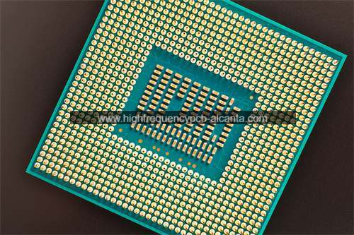
What is High Frequency packaging Substrate?
High Frequency packaging Substrate Manufacturer,High frequency packaging substrates are essential components in RF and microwave systems, facilitating the integration and interconnection of semiconductor devices. These substrates offer exceptional electrical properties, including low dielectric constants and minimal signal loss, ensuring efficient signal transmission at high frequencies. Typically made from materials like ceramics, organic laminates, or advanced composites, high frequency packaging substrates provide reliable mechanical support and thermal management. They are widely used in telecommunications, aerospace, and automotive industries, where high-speed data transmission and signal integrity are critical. Their precise construction and superior electrical performance enable the development of compact and high-performance electronic assemblies for various applications.
Specialized in the construction of electronic packages and interconnects, high-frequency packaging substrates cater specifically to devices operating within the radio frequency (RF) and microwave spectrums. They assume a critical function in maintaining the integrity and efficiency of signals, spanning applications like RF modules, communication systems, radar systems, and high-speed data transmission.
These substrates stand out for their ability to reduce signal attenuation and distortion. Marked by low loss, exceptional signal integrity, and high thermal conductivity, they play a vital role in ensuring the dependability of high-frequency signals. The importance of these substrates is emphasized by the increasing need for elevated data transfer rates and the widespread adoption of wireless communication technologies.
Materials commonly employed in high-frequency packaging substrates encompass specialized laminates, ceramics, and specific polymer types. The selection of these materials hinges on their capacity to deliver low dielectric loss, high thermal conductivity, and steadfast electrical properties across diverse frequencies. Employing advanced manufacturing techniques ensures meticulous control over dimensions and impedance matching.
The applications of high-frequency packaging substrates span a spectrum of electronic components, including antennas, power amplifiers, and filters. The choice of substrate material is contingent upon factors like operating frequency, power levels, and thermal considerations.
In essence, high-frequency packaging substrates play an indispensable role in the fabrication of electronic devices navigating the RF and microwave realms. Their distinctive attributes contribute to the dependable transmission of signals in high-speed scenarios, advancing communication systems and associated technologies
High Frequency packaging Substrate Manufacturer
How Does High-Frequency Packaging Substrate Enhance Electronic Systems?
At the core of electronic systems, the High-Frequency Packaging Substrate assumes a crucial role in significantly enhancing overall performance. Serving as a foundational support and interconnection framework for high-frequency electronic components, this substrate plays a pivotal role in maximizing both electrical performance and thermal management in advanced applications.
At its core function, the High-Frequency Packaging Substrate excels in minimizing signal attenuation and distortion, thereby safeguarding the integrity of high-frequency signals. Boasting attributes such as low loss, superior signal integrity, and high thermal conductivity, the substrate serves as a reliable medium for the seamless transmission of signals within the radio frequency (RF) and microwave ranges. Its exceptional characteristics make it a dependable and efficient conduit for preserving the accuracy and fidelity of high-frequency signals in electronic systems. This is particularly vital in applications like RF modules, communication systems, radar systems, and high-speed data transmission, where signal accuracy is paramount.
The substrate’s advanced design principles and meticulous material selection enable it to adeptly address the challenges presented by modern electronic communication systems. Offering precise control over dimensions and impedance matching, it facilitates optimal electrical performance, thereby contributing to the efficiency and reliability of the electronic system.
Furthermore, the High-Frequency Packaging Substrate assumes a crucial role in proficient thermal management within electronic systems. Its notable high thermal conductivity becomes instrumental in efficiently dissipating heat, effectively addressing and minimizing the risk of overheating issues in high-frequency electronic components. This thermal regulation is particularly essential to ensure the sustained and reliable performance of these components, contributing to the overall effectiveness of the electronic system.This is especially critical in applications where thermal stability is essential for sustained and reliable performance.
In summary, High-Frequency Packaging Substrate significantly enhances electronic systems by serving as a reliable foundation for supporting and interconnecting high-frequency components. Its contributions to signal integrity, electrical performance, and thermal management make it a critical and versatile element, ensuring the efficiency and reliability of diverse electronic applications.
What Diverse Materials Power High-Frequency Packaging Substrate?
High-Frequency Packaging Substrates utilize a varied selection of materials to address the intricate requirements of high-frequency electronic devices. This diverse array of materials is chosen strategically to optimize the performance and functionality of these substrates in the context of high-frequency applications.Different substrate types showcase unique characteristics tailored for specific applications within this domain.
Specialized laminates, often incorporating materials like polytetrafluoroethylene (PTFE), are widely adopted for their low dielectric loss properties.Substrates based on polytetrafluoroethylene (PTFE), exemplified by the Rogers RO4000 series, demonstrate exceptional performance in applications where superior signal integrity is paramount. Specifically, these substrates excel in high-demand scenarios such as RF amplifiers and antennas.
Ceramic materials, notably alumina (Al2O3) and aluminum nitride (AlN), are esteemed for their exceptional thermal conductivity. These substrates excel in scenarios where effective heat dissipation is paramount, playing a pivotal role in applications such as power amplifiers and high-frequency transducers. Their ability to efficiently manage heat contributes significantly to the optimal performance and reliability of electronic components in these specific high-frequency applications.
Certain polymer types, like liquid crystal polymer (LCP), strike a balance between electrical performance and cost-effectiveness. LCP substrates find application in high-frequency connectors, antennas, and packaging for wireless communication devices.
Each material is meticulously chosen to align with the specific requirements of the electronic device. PTFE-based substrates excel in scenarios demanding low loss and high signal integrity, ceramics are vital in situations requiring effective thermal management, and polymers offer a compromise between performance and cost.
In summary, the diverse materials propelling High-Frequency Packaging Substrates cater to a wide spectrum of applications. Each material type is carefully selected based on its unique characteristics, ensuring optimal performance in various high-frequency electronic devices while minimizing redundancy.
How Does High-Frequency Packaging Substrate Synergize with IC Package Technologies?.
High-Frequency Packaging Substrate serves as the foundational platform for mounting and interconnecting various electronic components, prominently including ICs. Its crucial role in ensuring signal integrity, efficient thermal management, and superior electrical performance cannot be overstated. The collaborative integration between the substrate and IC packaging technologies ensures a seamless synergy, facilitating the efficient transmission of high-frequency signals.
This cooperative relationship stands as a cornerstone for achieving optimal performance in electronic devices operating within the high-frequency spectrum. The meticulous interplay between High-Frequency Packaging Substrate and IC packaging technologies is central to the success and efficiency of electronic systems in the high-frequency domain.
IC packaging technologies, ranging from traditional dual in-line packages (DIP) to advanced ball grid arrays (BGA) and chip-on-board (COB) configurations, play a crucial role in encapsulating and protecting ICs. The choice of packaging technology impacts signal propagation and thermal characteristics. This aligns with the objectives of High-Frequency Packaging Substrate, as it must complement and enhance the performance of the chosen IC package.
The classifications of chip package technologies emphasize the need for tailored solutions in high-frequency applications. For instance, BGA packages provide enhanced thermal performance, which aligns well with substrates designed for effective heat dissipation in high-frequency power amplifiers.
In summary, the synergy between High-Frequency Packaging Substrate and IC packaging technologies is fundamental in achieving optimal performance in high-frequency electronic devices. The choice and design of IC packaging directly influence the interconnection and collaboration with the substrate, emphasizing the importance of a cohesive approach for successful high-frequency applications.
How Does High-Frequency Packaging Substrate Differ from Traditional PCBs?
Distinguishing themselves significantly from traditional Printed Circuit Boards (PCBs), high-frequency packaging substrates exhibit key differences, especially in applications such as motherboards, substrate-like PCBs, and High-Density Interconnect (HDI) substrates. These variances encompass material characteristics, signal integrity, data transmission speed, miniaturization capabilities, thermal performance, manufacturing precision, and cost considerations.
Material Selection: High-frequency substrates use specialized materials with low dielectric constants and minimal loss, optimizing signal integrity. Traditional PCBs typically rely on standard FR-4 materials that may not perform as well at higher frequencies.
Signal Integrity: High-frequency substrates excel in maintaining signal integrity, reducing signal loss and distortion. This is vital for applications such as motherboards where data transmission quality is essential, a challenge that traditional PCBs may face at high frequencies.
Data Transmission Speed: In applications like motherboards and HDI substrates, high-frequency substrates facilitate high-speed data transmission due to superior signal integrity and reduced electromagnetic interference. Traditional PCBs may struggle to match this performance.
Miniaturization: High-frequency substrates are better suited for miniaturization and high-density designs, allowing for compact layouts in motherboards and HDI substrates. Traditional PCBs may encounter difficulties achieving comparable miniaturization.
Thermal Performance: High-frequency substrates often offer enhanced thermal performance, crucial for dissipating heat in densely packed electronic components. This is especially relevant for motherboards, where traditional PCBs may not provide the same level of thermal management.
Cost Dynamics: High-frequency substrates may incur higher costs due to specialized materials and manufacturing processes. However, the enhanced performance often justifies the expense, especially in applications where high frequencies and data integrity are critical.
In summary, high-frequency packaging substrates distinguish themselves through material selection, superior signal integrity, high-speed data transmission capabilities, suitability for miniaturization, enhanced thermal performance, advanced manufacturing techniques, and, in some cases, a higher cost justified by improved performance in critical applications.
What Intricate Structures and Technologies Power High-Frequency Packaging Substrate?
High-frequency packaging substrates achieve their advanced electronic packaging capabilities through a combination of intricate structures and cutting-edge production technologies. Key processes include Improved HDI fabrication, which enhances substrate density through methods like laser drilling and precise alignment, enabling densely packed components for high-frequency applications. The Improved Semi-Additive method allows selective deposition of conductive materials, ensuring precise circuit patterns and minimizing signal distortion.
These substrates also employ specialized dielectric materials such as PTFE and liquid crystal polymers, chosen for their low dissipation factors and minimal signal loss. Advanced lamination techniques ensure uniform material properties, contributing to consistent electrical performance. Embedded passive components, integrated directly into the substrate, optimize space utilization and enhance overall circuit performance.
The use of high-precision etching processes enables the creation of intricate circuit patterns with tight tolerances, while controlled impedance design minimizes reflections and signal distortion. Microvia technology, involving tiny, high-density interconnects, reduces layer-to-layer spacing, enhancing signal transition times and overall signal integrity.
In essence, the sophisticated structures and technologies encompassed by high-frequency packaging substrates, such as Improved HDI fabrication, the Improved Semi-Additive method, specialized dielectric materials, embedded passive components, advanced material lamination, high-precision etching, controlled impedance design, and microvia technology, collectively propel them to the forefront of electronic packaging for high-frequency applications.
FAQs
How does it support emerging wireless applications?
Answer: High-frequency packaging substrate plays a crucial role in emerging wireless applications by providing a reliable platform for the construction of components that operate at higher frequencies. Its ability to minimize signal loss and maintain signal integrity is essential for the performance of devices in diverse wireless communication scenarios.
What manufacturing technologies contribute to the performance of High-Frequency Packaging Substrate?
Answer: Advanced manufacturing technologies such as Improved HDI fabrication, the Improved Semi-Additive method, specialized dielectric materials, embedded passive components, advanced material lamination, high-precision etching, controlled impedance design, and microvia technology contribute to the superior performance of high-frequency packaging substrates.
Can High-Frequency Packaging Substrate be used in miniaturized electronic devices?
Answer: Yes, high-frequency packaging substrates are well-suited for miniaturized electronic devices, offering designs conducive to compact layouts and high-density configurations. This adaptability makes them ideal for applications with limited space, such as emerging wireless technologies and compact consumer electronics.
What sets High-Frequency Packaging Substrate apart from traditional PCBs?
Distinctive features include material composition, signal integrity, thermal performance, and manufacturing techniques. High-frequency substrates are optimized for superior signal transmission and miniaturization in high-frequency applications.
Can High-Frequency Packaging Substrate Pave the Way for Future Innovations?
High-Frequency Packaging Substrate goes beyond being a component; it serves as a catalyst for upcoming innovations in electronic systems. Its substantial impact on high-frequency electronics suggests a pathway for advancements that can redefine the capabilities of electronic systems. Positioned at the forefront of technological evolution, this technology is poised to play a crucial role in the future where electronic systems demand higher performance, efficiency, and reliability.
As we journey into the high-frequency domain, the versatile applications of High-Frequency Packaging Substrate become increasingly evident. Its role extends beyond current needs, signifying its crucial involvement in shaping the landscape of future technologies.High-Frequency Packaging Substrate is poised to play a significant role in the anticipated advancements in 6G communication, the Internet of Things (IoT), and emerging technologies. Its importance as a crucial component is expected to persist, ensuring its active participation in shaping the future landscape of these innovative technologies.
In the ever-advancing landscape of electronic technologies, the need for accelerated data transmission and improved system performance is escalating. High-Frequency Packaging Substrate, tailored to meet the demanding standards of high-frequency applications, is strategically positioned as a driving force behind a continual wave of innovations. It is not merely a current necessity but a harbinger of transformative changes that will define the trajectory of electronic systems in the future. Thus, our exploration concludes with a recognition of High-Frequency Packaging Substrate’s pivotal role in the ongoing evolution of technology.


