 Professional high frequency circuit board supplier

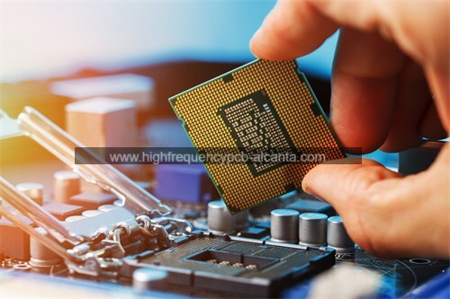
FCCSP Substrate Manufacturer
FCCSP Substrate Manufacturer,FCCSP (Flip Chip Chip-Scale Package) Substrates are advanced circuit boards designed for integrating flip chip components in a compact, high-performance package. These substrates feature a grid of solder bumps that directly connect the flip chip to the PCB, allowing for high-density interconnections and efficient electrical performance. FCCSP substrates are engineered to handle high-speed data transmission and offer excellent thermal management, making them ideal for applications in mobile devices, consumer electronics, and high-performance computing. Their compact design helps reduce the overall footprint of electronic devices while maintaining reliability and functionality in demanding environments.
What is an FCCSP Substrate?
An FCCSP substrate is a type of electronic component used in flip-chip packaging, which provides the base for connecting semiconductor devices to a circuit board. It’s designed to support high-density interconnections and thermal management for advanced electronic applications.An FCCSP (Flip Chip Chip Scale Package) Substrate is a type of substrate used in integrated circuit packaging, widely applied in high-performance, high-density, and compact electronic devices. It is a crucial component in modern electronic packaging technology, providing reliable electrical connections and mechanical support for advanced semiconductor chips.
FCCSP substrates are primarily made from organic materials such as BT resin or FR4, and inorganic materials like ceramics or silicon. The manufacturing process involves multilayer printed circuit board (PCB) technology, including precise photolithography, etching, and electroplating processes to achieve complex circuit patterns and high-density wiring. These substrates connect directly to the chip through tiny solder bumps, forming a Flip Chip structure, which facilitates the electrical interconnection between the chip and the substrate.
FCCSP substrates offer numerous advantages in modern electronic devices. Firstly, they support high-density integrated circuits, meeting the demand for increasingly miniaturized electronic products. Secondly, Flip Chip technology allows direct mounting of the chip onto the substrate, reducing signal transmission paths and significantly enhancing electrical performance and heat dissipation. Additionally, FCCSP substrates possess excellent mechanical strength and thermal stability, meeting the requirements of high-frequency and high-speed applications.
FCCSP substrates are widely used in fields such as mobile communications, computers, consumer electronics, and automotive electronics. For example, in smartphones, FCCSP substrates are used to package processors, memory, and other critical components, providing higher performance and smaller sizes. In automotive electronics, FCCSP substrates are used to package various sensors and control chips, enhancing system reliability and anti-interference capabilities.
In summary, FCCSP substrates, as an essential part of advanced packaging technology, continuously drive electronic products towards higher performance, smaller sizes, and greater reliability. Their exceptional electrical and mechanical properties make them indispensable materials in modern electronic packaging.
FCCSP Substrate Manufacturer
What are the FCCSP Substrate Design Guidelines?
FCCSP (Flip Chip Chip Scale Package) substrates are critical components in high-performance electronic packaging, and their design requires careful consideration to ensure optimal performance, reliability, and manufacturability. Here are key design guidelines for FCCSP substrates:
- Substrate Material Selection: Choose appropriate materials for the substrate, such as high-quality organic materials (BT resin or FR4) or inorganic materials (ceramics or silicon), depending on the electrical, thermal, and mechanical requirements of the application.
- Bump Design: Design the solder bumps with precision to ensure proper alignment and reliable electrical connections. The bump pitch, size, and composition must be optimized for the specific chip and substrate requirements.
- Thermal Management: Incorporate thermal vias and heat spreaders to manage heat dissipation effectively. Adequate thermal management is essential to prevent overheating and ensure the reliability of the electronic components.
- Electrical Performance: Ensure that the substrate design supports high-frequency signal transmission with minimal loss and interference. Use appropriate trace widths, spacing, and via designs to maintain signal integrity and reduce noise.
- Mechanical Stability: Design the substrate to provide sufficient mechanical support for the chip, ensuring stability during handling and operation. Consider the substrate’s mechanical properties to avoid warping or deformation.
- Layer Structure: Utilize a multi-layer design to accommodate complex circuit patterns and high-density interconnections. Ensure proper layer alignment and adhesion to achieve reliable performance.
- Manufacturability: Design the substrate with manufacturing constraints in mind. This includes considering factors like the ease of photolithography, etching, and plating processes. Minimize design features that could complicate manufacturing or increase costs.
- Reliability Testing: Incorporate design features that facilitate reliability testing and quality assurance. This includes designing test pads and test structures to verify the integrity and performance of the substrate.
- Environmental Considerations: Ensure the substrate design meets environmental standards and regulations. Consider factors such as thermal cycling, humidity, and chemical exposure to ensure long-term reliability.
- Size and Form Factor: Design the substrate to meet the specific size and form factor requirements of the end application. Ensure that the dimensions are compatible with the chip and the final packaging requirements.
By adhering to these design guidelines, engineers can create FCCSP substrates that deliver high performance, reliability, and manufacturability for advanced electronic applications.
What is the FCCSP Substrate Fabrication Process?
The FCCSP (Flip Chip Chip Scale Package) substrate fabrication process involves several critical steps to ensure the production of high-quality substrates suitable for advanced electronic packaging. Below is an overview of the key stages in the FCCSP substrate fabrication process:
- Material Preparation: Start with the selection and preparation of substrate materials, typically consisting of organic materials (such as BT resin or FR4) or inorganic materials (such as ceramics or silicon). These materials are chosen based on the electrical, thermal, and mechanical properties required for the application.
- Copper Foil Lamination:Apply a thin layer of copper foil to the substrate material using a lamination process. This copper layer will serve as the base for creating electrical circuits and interconnections on the substrate.
- Photolithography: Use photolithography to define the circuit patterns on the substrate. A photosensitive material (photoresist) is applied to the copper layer, and ultraviolet (UV) light is used to expose specific areas through a mask, creating a pattern that will guide the subsequent etching process.
- Etching: Remove the unprotected copper from the substrate using an etching solution, leaving behind the desired circuit patterns. This process creates the conductive pathways necessary for electrical connections.
- Plating and Deposition: Apply additional metal layers (such as gold or nickel) through electroplating or other deposition methods to enhance the electrical and mechanical properties of the substrate. This may include adding solder bumps or pads for flip-chip connections.
- Via Formation:Create vias (vertical electrical connections) through the substrate layers to enable multi-layer interconnections. This is typically done through drilling and subsequent plating processes to ensure reliable conductivity between layers.
- Solder Bump Formation: Deposit and reflow solder bumps onto the designated areas of the substrate. These solder bumps will connect directly to the flip-chip die, facilitating electrical and mechanical bonding.
- Dicing and Cutting: Cut the large substrate panels into individual substrates or dice them into smaller pieces as required. Precision cutting is essential to ensure that each substrate meets the desired specifications and dimensions.
- Inspection and Testing: Conduct thorough inspections and tests to verify the quality and performance of the substrates. This includes checking for defects, measuring electrical performance, and ensuring that the substrates meet design and manufacturing standards.
- Packaging and Delivery: Once the substrates pass inspection and testing, they are packaged and prepared for delivery to customers. Packaging must protect the substrates from damage during transport and handling.
By following these fabrication steps, manufacturers can produce high-quality FCCSP substrates that meet the rigorous demands of modern electronic applications. Each stage of the process is critical to ensuring the final product’s performance, reliability, and compatibility with advanced packaging technologies.
How Do You Manufacture an FCCSP Substrate?
The manufacturing of FCCSP (Flip Chip Chip Scale Package) substrates involves a series of precise steps to ensure the production of high-performance substrates suitable for advanced electronic packaging. Here’s a detailed overview of the manufacturing process:
- Material Selection and Preparation: Choose the appropriate substrate material, which could be organic (e.g., BT resin or FR4) or inorganic (e.g., ceramics or silicon). Prepare the material by cutting it to the required size and ensuring it is clean and free of contaminants.
- Copper Foil Lamination: Laminate a thin layer of copper foil onto the substrate material. This copper layer will serve as the base for the electrical circuits and interconnections. The lamination process involves heating and pressing the copper foil onto the substrate material.
- Photolithography: Apply a photosensitive resist layer to the copper-coated substrate. Use photolithography to expose the resist to ultraviolet (UV) light through a mask that defines the circuit patterns. This step creates a patterned resist layer that protects certain areas of the copper.
- Etching: Etch away the unprotected copper from the substrate using a chemical etching solution. The remaining copper forms the circuit patterns required for electrical connections. This process defines the conductive pathways on the substrate.
- Plating and Deposition: Apply additional metal layers to the substrate through electroplating or other deposition techniques. This step may include plating with materials such as gold or nickel to enhance the electrical and mechanical properties of the substrate.
- Via Formation: Create vias, which are vertical interconnections through the substrate layers. This involves drilling holes through the substrate and then plating the holes with metal to ensure reliable electrical connections between different layers.
- Solder Bump Formation: Deposit and reflow solder bumps onto specific areas of the substrate. These solder bumps will form the electrical and mechanical connections with the flip-chip die. The process involves applying solder paste, placing solder balls, and heating the substrate to reflow the solder into bumps.
- Inspection and Testing: Conduct thorough inspections and testing of the substrates to ensure they meet quality and performance standards. This includes checking for defects, measuring electrical performance, and verifying that the solder bumps are correctly formed and aligned.
- Dicing and Cutting: Cut the substrate panels into individual substrates or dice them into smaller pieces. Precision cutting is essential to achieve the desired dimensions and ensure each substrate meets the specifications.
- Final Inspection and Packaging: Perform a final inspection to ensure all substrates are defect-free and meet the required standards. Package the substrates carefully to protect them during transport and handling.
By following these manufacturing steps, FCCSP substrates can be produced with high precision and performance, making them suitable for advanced electronic applications requiring compact size, high-density interconnections, and excellent thermal and electrical properties.
How Much Should an FCCSP Substrate Cost?
The cost of an FCCSP (Flip Chip Chip Scale Package) substrate can vary widely based on several factors. Here’s a detailed overview of the elements that influence the cost of FCCSP substrates:
- Material Costs:The choice of substrate materials (organic or inorganic) significantly impacts the cost. High-performance materials such as ceramics or advanced organic laminates generally cost more than standard materials. The cost of raw materials, including copper foil and solder bump materials, also affects the overall cost.
- Design Complexity: The complexity of the circuit design, including the number of layers, the density of interconnections, and the precision required, influences the cost. More complex designs with finer features and tighter tolerances typically require more advanced manufacturing processes and, consequently, higher costs.
- Manufacturing Processes: The fabrication steps, including photolithography, etching, plating, and solder bump formation, contribute to the overall cost. Advanced processes, such as those required for high-frequency or high-density substrates, may increase manufacturing costs. The efficiency and scale of the production process also play a role.
- Volume and Scale: The cost per substrate can decrease with higher production volumes due to economies of scale. Bulk orders often benefit from lower per-unit costs, whereas small production runs may incur higher costs due to lower efficiencies and higher setup costs.
- Testing and Quality Assurance: Comprehensive testing and quality assurance processes ensure that substrates meet performance and reliability standards. The cost of inspection, testing, and validation adds to the overall cost of the substrate.
- Lead Time and Customization: Custom designs or expedited production may incur additional costs. The lead time required for production, including any rush orders or specialized requirements, can also impact the pricing.
- Geographic Location: Manufacturing costs can vary by region due to differences in labor costs, facility overhead, and local regulations. Substrate manufacturers located in regions with higher labor costs or stricter regulations may charge more for their products.
- Supplier and Market Conditions: Prices can fluctuate based on market conditions, supplier agreements, and availability of materials. Changes in the supply chain or material costs can affect substrate pricing.
In general, the cost of FCCSP substrates can range from a few dollars to several hundred dollars per unit, depending on the factors listed above. For example, simple, low-volume substrates might cost in the lower range, while high-performance, custom substrates with complex designs and rigorous testing might be on the higher end. To obtain an accurate cost estimate, it is essential to consult with substrate manufacturers, provide detailed design specifications, and consider production volumes and additional requirements.
What is FCCSP Substrate Base Material?
The base material of an FCCSP (Flip Chip Chip Scale Package) substrate is crucial for determining its performance, reliability, and suitability for high-density electronic applications. The base material serves as the foundation upon which electrical circuits and interconnections are built. Here’s an overview of the key base materials used in FCCSP substrates:
- Organic Materials:
– BT Resin (Bismaleimide-Triazine): BT resin is a widely used organic material for FCCSP substrates due to its excellent thermal stability, low moisture absorption, and good electrical insulation properties. It provides a stable platform for high-density interconnections and is suitable for high-performance applications.
– FR4 (Flame Retardant 4): FR4 is a commonly used material in PCB manufacturing, including FCCSP substrates. It is made from woven glass fabric impregnated with epoxy resin. While it offers good electrical insulation and mechanical strength, it has lower thermal performance compared to BT resin.
- Inorganic Materials:
– Ceramics: Ceramic materials, such as alumina (Al2O3) or aluminum nitride (AlN), are used in FCCSP substrates for their superior thermal conductivity, mechanical strength, and electrical insulation. Ceramics are ideal for high-power and high-frequency applications where efficient heat dissipation and stability are crucial.
– Silicon: Silicon is used in some advanced FCCSP substrates, particularly in silicon-based integrated circuit (IC) packaging. It offers excellent thermal and electrical properties and is well-suited for high-performance and high-density applications.
- Polyimide: Polyimide is another material used in FCCSP substrates for its excellent thermal stability, chemical resistance, and flexibility. It is often used in high-temperature applications and for substrates requiring a combination of mechanical strength and electrical performance.
- Composite Materials:Composite materials, which combine organic and inorganic components, can be used to tailor the substrate properties for specific applications. These materials may include combinations of resins, fillers, and reinforcements to achieve desired thermal, electrical, and mechanical characteristics.
The choice of base material for FCCSP substrates depends on factors such as the application’s thermal and electrical requirements, mechanical properties, and cost considerations. Each material offers distinct advantages and trade-offs, making it essential to select the appropriate base material based on the specific needs of the electronic device and its operating environment.
Which Company Makes FCCSP Substrates?
Currently, several companies manufacture FCCSP (Flip Chip Chip Scale Package) substrates, including Anpec, TSMC (Taiwan Semiconductor Manufacturing Company), UMC (United Microelectronics Corporation), Intel, and TSMC (Taiwan Semiconductor Manufacturing Company). These companies possess advanced technologies and equipment, enabling them to produce high-performance FCCSP substrates widely used in semiconductor chip packaging, mobile communications, computing, and consumer electronics.
Anpec is renowned for its high-precision packaging solutions, with its FCCSP substrates having broad applications in high-performance and high-density packaging. TSMC, as a global leader in semiconductor manufacturing, provides advanced FCCSP packaging technologies to meet various high-performance chip requirements. UMC focuses on producing highly reliable FCCSP substrates, offering stable packaging solutions to customers. Intel has extensive experience in FCCSP packaging technology, providing efficient packaging services for its processors and other chips. TSMC also has substantial technical expertise and production capability in FCCSP substrates, delivering high-quality packaging solutions to global customers.
Our company also has the capability to manufacture FCCSP substrates. Our products use high-performance base materials to ensure excellent performance under high-density packaging conditions. Our FCCSP substrates have the following features:
- Superior High-Density Packaging Performance: We use high-quality base materials, such as reliable organic and ceramic materials, ensuring stability and high performance of the FCCSP substrates in high-density packaging.
- High Precision Processing: Our company has advanced processing equipment and a skilled technical team, enabling high-precision circuit processing and lamination to ensure high product quality.
- Multi-Layer Structure Design: We can design and manufacture multi-layer FCCSP substrates based on customer needs, meeting the requirements of complex circuit applications.
- High-Quality After-Sales Service: We provide comprehensive after-sales service to ensure customers receive timely technical support and solutions during use.
- Customized Services: We offer customized FCCSP substrate design and manufacturing services based on specific customer requirements, ensuring products fully meet application needs.
Through continuous technological innovation and rigorous quality control, our FCCSP substrates are widely recognized in the market and are applied in semiconductor packaging, communications, computing, and other high-performance fields. If you have FCCSP substrate needs, please contact us, and we will provide you with high-quality products and services.
In summary, whether it is material selection, processing technology, or after-sales service, our company is capable of producing high-quality FCCSP substrates to meet the needs of various high-performance applications.
What are the 7 Qualities of Good Customer Service?
Good customer service is essential for building strong relationships with customers and ensuring their satisfaction. Here are seven key qualities that define excellent customer service:
- Promptness: Providing quick and efficient responses to customer inquiries and issues is crucial. Promptness shows respect for the customer’s time and helps resolve problems swiftly, enhancing overall satisfaction.
- Courtesy: Treating customers with respect and politeness is fundamental. Courtesy involves being friendly, considerate, and empathetic, which helps create a positive and welcoming interaction.
- Knowledgeability: Customer service representatives should have a deep understanding of the products or services offered. Being knowledgeable allows them to provide accurate information, answer questions effectively, and offer relevant solutions.
- Communication Skills: Effective communication is key to good customer service. This includes not only clear and concise verbal communication but also active listening, understanding customer needs, and providing helpful responses.
- Problem-Solving Abilities: Good customer service involves the ability to handle and resolve issues efficiently. Representatives should be adept at identifying problems, thinking critically, and providing practical solutions to meet customer needs.
- Empathy: Showing empathy means understanding and acknowledging the customer’s feelings and experiences. Empathetic service helps build trust and rapport, making customers feel valued and understood.
- Follow-Up: Ensuring that customer issues are resolved and following up to confirm satisfaction is important. Follow-up demonstrates commitment to customer care and helps ensure that any outstanding issues are addressed appropriately.
These qualities collectively contribute to a positive customer experience, fostering loyalty and encouraging repeat business. By focusing on promptness, courtesy, knowledgeability, communication skills, problem-solving abilities, empathy, and follow-up, companies can deliver exceptional customer service and build lasting relationships with their customers.
FAQs about FCCSP Substrates
What is the main advantage of using FCCSP substrates?
FCCSP substrates offer high-density interconnections, excellent thermal performance, and compact packaging, making them ideal for advanced electronic applications.
How do I choose the right FCCSP substrate for my application?
Consider factors such as electrical performance, thermal management, mechanical strength, and compatibility with your design requirements when selecting a substrate.
What is the typical lead time for FCCSP substrate manufacturing?
Lead times can vary based on complexity and order volume. It’s best to check with the manufacturer for specific timeframes.
Can FCCSP substrates be customized?
Yes, FCCSP substrates can be customized to meet specific design and performance criteria.