What is Extra Small Pitch High Frequency PCB?
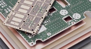
Extra Small Pitch High Frequency PCB Supplier,Extra small pitch high-frequency PCBs are specialized substrates designed for compact electronic devices requiring precise signal transmission. With smaller pitch sizes, typically less than 100 micrometers, these PCBs enable high-density interconnections and miniaturization. They feature advanced materials with exceptional electrical properties, ensuring minimal signal loss and high-speed data transmission. Extra small pitch high-frequency PCBs find applications in industries such as telecommunications, automotive, and IoT devices, where space-saving and reliable performance are paramount. Their compact design and superior electrical characteristics make them indispensable for modern electronics, facilitating the development of smaller and more efficient electronic systems.
Extra Small Pitch High-Frequency PCBs, or ESPHF PCBs, stand out as a specialized category of printed circuit boards tailored to the demanding needs of high-frequency applications in the electronics industry. These boards play a crucial role in cutting-edge technologies such as telecommunications, aerospace, and wireless communication systems.
Distinguished by their closely spaced arrangement of components and traces, ESPHF PCBs feature a significantly smaller pitch compared to standard PCBs. This compact design is essential for enhancing signal integrity and minimizing signal loss, particularly at higher frequencies.
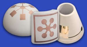
The high-frequency characteristics of ESPHF PCBs are essential for applications operating in the radio frequency (RF) or microwave range. Traditional PCBs often face challenges like signal degradation and electromagnetic interference at these frequencies. ESPHF PCBs overcome these issues by utilizing carefully chosen substrate materials with low dielectric constant and loss tangent to reduce signal attenuation. Materials such as Rogers 4000 series and high-frequency laminates with improved electrical properties are commonly employed.
The increasing demand for ESPHF PCBs is driven by technological progress and the widespread adoption of high-frequency applications. Industries such as 5G communication, radar systems, and satellite communication heavily rely on these PCBs to meet their performance requirements.
Moreover, the prevalent trend of miniaturization in electronics, fueled by the quest for smaller and lighter devices, has heightened the importance of Extra Small Pitch High-Frequency PCBs. Their compact design and precise component placement empower manufacturers to create smaller yet more efficient electronic devices without compromising performance.
To sum up, Extra Small Pitch High-Frequency PCBs play a vital role in the evolution of high-frequency electronic systems. Their distinct design, characterized by closely spaced components and specialized substrate materials, positions them as ideal solutions for applications where signal integrity and minimal signal loss are paramount. As technology advances, the demand for ESPHF PCBs is expected to grow, influencing the trajectory of high-frequency electronics.

Extra Small Pitch High Frequency PCB Supplier
Functions of Extra Small Pitch High Frequency PCB
Extra Small Pitch High Frequency PCBs play a vital role in high-frequency electronic devices, offering a platform for seamless integration of electronic components. Specifically tailored for applications like communication systems, radar, and RF transmission, these PCBs serve the following key functions:
Signal Integrity Enhancement:
An essential function is optimizing signal integrity. The reduced pitch allows for precise routing of high-frequency signals, minimizing issues like signal loss, crosstalk, and impedance mismatch.
This is particularly crucial in communication systems and radar applications where dependable signal transmission is paramount.
Optimized High-Frequency Performance:
Tailored for high-frequency applications, these PCBs excel in accommodating the unique requirements of such devices. The smaller pitch enables tighter trace spacing, contributing to improved high-frequency performance.
Devices in RF transmission benefit from these PCBs, which can handle fast signal switching and high data rates effectively.
Parasitic Capacitance and Inductance Reduction:
Minimizing parasitic capacitance and inductance between traces and components is facilitated by the smaller pitch. In high-frequency circuits, any additional capacitance or inductance can be detrimental to performance.
Reduced parasitic elements enhance the efficiency and reliability of high-frequency electronic devices.
Precision Impedance Control:
These PCBs allow for accurate control of trace impedance, a critical aspect in RF transmission systems. Maintaining specific impedance across the circuit is essential for optimal signal transfer and reception.
Accurate impedance control minimizes signal reflections, ensuring transmitted signals align with connected devices’ impedance.
Facilitating Miniaturization:
The smaller pitch supports the miniaturization of electronic devices, a key requirement in radar applications. Compact and lightweight components are essential for mobility and efficient performance.
Miniaturization contributes to reducing the overall size and weight of communication systems, enhancing their versatility.
Specialized Material Selection:
Extra Small Pitch High Frequency PCBs often employ materials with high dielectric constants and low loss tangents to meet high-frequency signal demands. Material selection is critical for optimal electrical performance.
These materials contribute to maintaining low signal loss and preserving signal quality in high-frequency applications.
Efficient Thermal Management:
Ensuring effective heat dissipation is crucial, especially in high-power applications. These PCBs may incorporate advanced thermal management techniques to dissipate heat generated during operation.
This is vital in RF transmission systems with high-power amplifiers, ensuring the reliability and longevity of electronic components.
In essence, Extra Small Pitch High Frequency PCBs are tailored to meet the demanding requirements of high-frequency electronic devices. Their functions include enhancing signal integrity, optimizing high-frequency performance, reducing parasitic elements, ensuring precise impedance control, facilitating miniaturization, employing specialized materials, and implementing efficient thermal management. These features collectively make them indispensable in communication systems, radar, and RF transmission applications.
Different Types of Extra Small Pitch High Frequency PCBs
Exploring Diverse Extra Small Pitch High-Frequency PCB Types:
Microstrip PCBs:
Features: Microstrip PCBs, characterized by a thin conductor on one side and dielectric material, offer precise impedance control with an extra small pitch.
Benefits: Ideal for applications demanding controlled impedance, commonly utilized in high-frequency circuits and microwave systems.
Applicability: Well-suited for scenarios where precise signal integrity matters, such as in radar systems and satellite communication.
Stripline PCBs:
Features: Stripline PCBs have conductive traces between dielectric layers, ensuring high isolation and reduced electromagnetic interference due to closely spaced components.
Advantages: Suited for applications requiring minimal crosstalk, often found in RF filters and high-frequency communication devices.
Applicability: Effective in scenarios where signal isolation is crucial, as seen in RF communication systems and wireless networks.
Coaxial PCBs:
Features: Coaxial PCBs incorporate a central conductor surrounded by a dielectric layer and outer conductor, ensuring efficient signal transmission with a controlled pitch.
Benefits: Known for superior signal integrity and low radiation, commonly used in high-frequency measurement equipment and data transmission systems.
Applicability: Ideal for situations prioritizing minimal signal loss and precise impedance control, like in high-frequency test and measurement devices.
Embedded PCBs:
Features: Embedded PCBs have components mounted between layers, contributing to a compact design with an extra small pitch.
Advantages: Suited for space-constrained applications, frequently employed in compact electronics like smartphones and wearables.
Applicability: Ideal for scenarios emphasizing size reduction and high component density, such as in consumer electronics and portable communication devices.
Multilayer PCBs:
Features: Multilayer PCBs consist of multiple conductive trace and dielectric layers, offering increased circuit density and reduced electromagnetic interference with an extra small pitch.
Benefits: Provide flexibility in routing and reduced electromagnetic interference, commonly used in high-density electronic applications.
Applicability: Well-suited for scenarios requiring high component density and complex circuitry, including high-performance computing and advanced signal processing systems.
Understanding the nuances of each Extra Small Pitch High-Frequency PCB type enables informed decision-making when selecting the most suitable option based on specific application requirements. The diverse features and benefits cater to a broad spectrum of needs within the realm of high-frequency electronics.
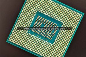
Extra Small Pitch High Frequency PCBs and IC Packaging
Diverse IC Packaging Technology Classifications:
Through-Hole Technology (THT):
Overview: THT, a traditional packaging method, involves component mounting through holes in the PCB, enhancing its versatility.
Role: While THT serves various applications, its larger pitch may pose challenges for high-frequency circuits requiring meticulous signal integrity.
Surface Mount Technology (SMT):
Overview: SMT simplifies manufacturing by placing components directly onto the PCB surface, promoting efficiency.
Role: Although SMT accommodates finer pitches, it may encounter limitations in achieving ultra-tight pitches, particularly for Extra Small Pitch High-Frequency PCBs.
Ball Grid Array (BGA):
Overview: BGA packages, featuring a solder ball array beneath, offer notable thermal and electrical benefits.
Role: While BGA enhances thermal performance, its pitch may not always align with the ultra-small dimensions required for high-frequency applications.
Flip-Chip Technology:
Overview: In flip-chip packaging, the IC is inverted, and solder bumps establish direct connections with the PCB.
Role: Flip-chip technology, with its finer pitches, aligns well with the requirements of Extra Small Pitch High-Frequency PCBs.
The Integral Role of Extra Small Pitch High-Frequency PCBs:
Extra Small Pitch High-Frequency PCBs act as a vital link in the chain of chip packaging technology, providing a substrate that accommodates the ultra-tight pitches crucial for high-frequency applications. Tailored with materials featuring low dielectric constant and loss tangent, these PCBs ensure minimal signal attenuation at elevated frequencies.
The meticulous arrangement of components on Extra Small Pitch High-Frequency PCBs seamlessly complements advanced IC packaging techniques. Whether it’s the precision demanded by flip-chip technology or the intricacies of advanced BGA configurations, these PCBs play a pivotal role in facilitating the seamless integration of high-frequency ICs into electronic systems.
In essence, the symbiosis between Extra Small Pitch High-Frequency PCBs and IC packaging technology is fundamental to the advancement of high-performance electronic devices. By providing the required substrate for ultra-small pitches, these PCBs empower the evolution of telecommunications, wireless communication, and other high-frequency applications.
Comparison of Extra Small Pitch High Frequency PCBs with Traditional PCBs
Comparative Analysis: Extra Small Pitch High-Frequency PCBs vs. Traditional PCBs, Motherboards, SLPs, and HDI Boards
In the landscape of electronic circuitry, a nuanced comparison between Extra Small Pitch High-Frequency PCBs and their counterparts, including traditional PCBs, motherboards, Substrate-Like PCBs (SLPs), and High-Density Interconnect (HDI) boards, sheds light on their distinctive advantages in high-frequency applications.
Traditional PCBs:
Overview: Conventional PCBs serve as the baseline, featuring standard pitch and component arrangement.
Comparison: Extra Small Pitch High-Frequency PCBs excel in high-frequency scenarios due to their closely spaced components, minimizing signal loss and interference.
Motherboards:
Overview: Motherboards are complex, integrating various functionalities with a mix of standard and high-frequency components.
Comparison: Extra Small Pitch High-Frequency PCBs offer targeted advantages in specific high-frequency applications, ensuring superior signal integrity where critical.
Substrate-Like PCBs (SLPs):
Overview: SLPs mimic the properties of semiconductor substrates, providing enhanced electrical performance.
Comparison: Extra Small Pitch High-Frequency PCBs, with their fine pitch, further optimize signal integrity, making them ideal for applications demanding precise control over high frequencies.
High-Density Interconnect (HDI) Boards:
Overview: HDI boards leverage advanced interconnect technologies for increased component density.
Comparison: While HDI boards enhance overall density, Extra Small Pitch High-Frequency PCBs specifically target high-frequency needs with their optimized design for minimal signal attenuation.
Advantages of Extra Small Pitch High-Frequency PCBs in High-Frequency Applications:
Precision in Signal Integrity:
Extra Small Pitch High-Frequency PCBs: Their fine pitch ensures precise control over signal integrity, reducing signal loss and interference at high frequencies.
Optimized for High Frequencies:
Extra Small Pitch High-Frequency PCBs: Tailored for applications operating in the radio frequency (RF) or microwave range, ensuring optimal performance.
Reduced Electromagnetic Interference:
Extra Small Pitch High-Frequency PCBs: Closely spaced components contribute to minimized electromagnetic interference, critical in high-frequency environments.
Compact Design and Miniaturization:
Extra Small Pitch High-Frequency PCBs: Ideal for compact and lightweight electronic devices, supporting the broader trend of miniaturization in the industry.
Specialized Material Selection:
Extra Small Pitch High-Frequency PCBs: Engineered with materials like Rogers 4000 series or high-frequency laminates to minimize dielectric losses at high frequencies.
In summary, the comparison highlights that Extra Small Pitch High-Frequency PCBs outshine traditional PCBs, motherboards, SLPs, and HDI boards in specific high-frequency applications. Their fine pitch, optimized design, and specialized material selection position them as key players in advancing technologies that rely on superior signal integrity and minimal signal attenuation at elevated frequencies.
Structure and Production Technologies of Extra Small Pitch High Frequency PCBs
Navigating the Intricacies of Extra Small Pitch High-Frequency PCBs: Structure and Innovative Production Techniques
Architecture of Extra Small Pitch High-Frequency PCBs:
Precision in Component Arrangement:
Extra Small Pitch High-Frequency PCBs distinguish themselves through closely spaced components, enabling ultra-fine pitches. This meticulous layout is pivotal for achieving impeccable signal integrity in high-frequency applications.
Tailored Substrate Materials:
Carefully chosen substrate materials, featuring low dielectric constant and loss tangent, such as Rogers 4000 series or high-frequency laminates, contribute to minimizing signal attenuation. This ensures efficient signal transmission at elevated frequencies.
Multilayer Configurations:
A common feature involves adopting a multilayer design, incorporating multiple conductive and dielectric layers. This design not only enhances circuit density but also mitigates electromagnetic interference, addressing the intricate demands of high-frequency electronic systems.
Progressive Manufacturing Techniques:
Enhanced HDI Processes:
High-Density Interconnect (HDI) manufacturing undergoes enhancements to seamlessly adapt to the fine pitches and heightened component density of Extra Small Pitch High-Frequency PCBs. Integration of microvias, fine-line traces, and multiple layers contributes to elevating performance standards.
Innovative Semi-Additive Approaches:
Semi-additive methods revolutionize the production landscape by selectively introducing copper to specific areas on the substrate. This precision is fundamental in crafting ultra-fine features, aligning with the closely spaced components characteristic of Extra Small Pitch High-Frequency PCBs.
Laser Direct Imaging (LDI) Techniques:
Laser Direct Imaging (LDI) takes the forefront for precise photoresist exposure, ensuring intricate patterns on the PCB. This technology is instrumental in achieving the fine details indispensable for the small pitches characteristic of Extra Small Pitch High-Frequency PCBs.
Controlled Impedance Matching Expertise:
Advanced manufacturing technologies empower precise control over impedance matching, a critical consideration in high-frequency applications. This capability ensures that signals propagate with minimal distortion and loss, meeting the stringent requirements of contemporary electronic systems.
In Conclusion:
Extra Small Pitch High-Frequency PCBs emerge as pioneers in technological sophistication, boasting intricate structures and employing cutting-edge manufacturing techniques. The meticulous component arrangement, strategic substrate material selection, and incorporation of advanced manufacturing methodologies collectively contribute to their exceptional performance in high-frequency applications. As technology continues its trajectory, these PCBs remain at the forefront, shaping the landscape of high-frequency electronics.
FAQs about Extra Small Pitch High Frequency PCBs
How does the multilayer design benefit Extra Small Pitch High-Frequency PCBs in high-frequency applications?
The multilayer design enhances circuit density, mitigates electromagnetic interference, and meets the complex requirements of high-frequency electronic systems. It enables precise control over impedance matching, facilitating optimal signal propagation.
What are the advanced manufacturing techniques used for Extra Small Pitch High-Frequency PCBs?
Advanced manufacturing techniques encompass enhanced High-Density Interconnect (HDI) processes, innovative semi-additive methods, and Laser Direct Imaging (LDI). These techniques ensure precise creation of ultra-fine features, aligning with the small pitches characteristic of Extra Small Pitch High-Frequency PCBs.
In which applications are Extra Small Pitch High-Frequency PCBs commonly employed?
Extra Small Pitch High-Frequency PCBs find applications in high-frequency electronic systems such as 5G communication, radar systems, satellite communication, and other wireless technologies. Their optimal signal integrity is essential for scenarios where high-frequency performance is critical.
What is the significance of controlled impedance matching in Extra Small Pitch High-Frequency PCBs?
Controlled impedance matching is crucial in Extra Small Pitch High-Frequency PCBs to ensure minimal signal distortion and loss during propagation. This feature is essential for meeting the stringent requirements of high-frequency applications where precise signal integrity is paramount.
8. Conclusion
As we bring our exploration of Extra Small Pitch High-Frequency PCBs to a close, it’s evident that these specialized circuit boards stand as pioneers in the realm of technological innovation, particularly within high-frequency applications. The distinct design, characterized by closely arranged components and thoughtfully chosen substrate materials, rises to meet the intricate challenges presented by signals at elevated frequencies.
The inherent multilayer design of Extra Small Pitch High-Frequency PCBs not only enhances circuit density but also acts as a shield against electromagnetic interference. This makes them indispensable for integration into advanced electronic systems. Embracing cutting-edge manufacturing technologies, including refined High-Density Interconnect (HDI) processes and inventive semi-additive methods, underscores a dedication to achieving precision and efficiency in their production.
As we address commonly raised questions, it becomes apparent that these PCBs play a pivotal role in propelling the progress of high-frequency electronics. Their contributions, spanning improved signal integrity, minimized interference, and support for device miniaturization, seamlessly align with the evolving needs of the electronics industry.
In summary, Extra Small Pitch High-Frequency PCBs serve as a testament to the ceaseless pursuit of excellence in electronics design. Their evolutionary trajectory not only defines the current landscape but also charts a course for future breakthroughs in high-frequency applications. Positioned at the forefront of technological advancement, these PCBs are poised to continue their instrumental role in the unfolding narrative of electronic innovation.
 Professional high frequency circuit board supplier


