 Professional high frequency circuit board supplier
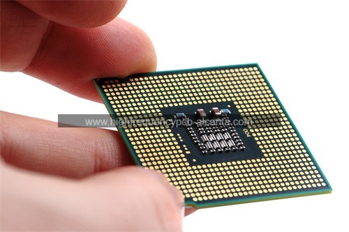
What is DIP Package Substrate?
DIP Package Substrate Manufacturer,DIP (Dual In-line Package) substrate is a classic semiconductor packaging format known for its simplicity and versatility. Featuring two parallel rows of leads extending from its body, DIP substrates offer easy assembly and robust mechanical support. They ensure reliable electrical connections and are suitable for various electronic applications, from consumer electronics to industrial equipment. DIP package substrates provide excellent thermal management and signal integrity, making them ideal for high-reliability applications. Their straightforward design and compatibility with through-hole assembly processes make DIP substrates a preferred choice for many electronic designs requiring durability and ease of use.
A DIP (Dual Inline Package) substrate refers to the physical material upon which the integrated circuit (IC) or electronic component is mounted in a dual inline package. The substrate serves as a foundation for the IC or component, providing mechanical support as well as electrical connections between the device and the circuit board it’s mounted on.
DIP packages are a type of through-hole mounting method where the leads of the package are inserted into holes in the circuit board and soldered to provide both mechanical and electrical connection. The substrate typically consists of a rigid material such as fiberglass-reinforced epoxy resin (FR4) or ceramic, which provides structural integrity and electrical insulation.
The DIP substrate also often includes conductive traces or pads to facilitate the connection between the leads of the IC or component and the external circuitry on the circuit board. These traces or pads are typically made of copper and are patterned onto the substrate using techniques such as etching or printing.
Overall, the DIP package substrate plays a crucial role in ensuring the mechanical stability and electrical connectivity of the IC or electronic component within the circuit assembly.
DIP Package Substrate Manufacturer
What are the Functions of DIP Package Substrate?
The DIP (Dual Inline Package) package substrate serves several important functions:
Mechanical Support: The substrate provides a stable platform for mounting the integrated circuit (IC) or electronic component. It ensures that the device is securely held in place within the package, preventing physical damage or displacement during handling, assembly, or operation.
Electrical Interconnection: The substrate facilitates electrical connections between the IC or component and the external circuitry on the printed circuit board (PCB). This is typically achieved through conductive traces or pads on the substrate, which link the leads of the device to corresponding points on the PCB, enabling the flow of electrical signals between the IC/component and other parts of the circuit.
Heat Dissipation: In some cases, the substrate may also play a role in dissipating heat generated by the IC or component during operation. This is particularly important for high-power devices or those operating in demanding environments where heat buildup can affect performance or reliability. The substrate material may have thermal properties optimized for efficient heat transfer, or additional heat sink structures may be incorporated into the package design.
Electrical Isolation: The substrate acts as an electrical insulator, preventing short circuits or unintended electrical interactions between the leads of the IC/component and the conductive elements of the PCB. This isolation ensures proper functionality and reliability of the device within the circuit assembly.
Environmental Protection: The substrate may provide a degree of protection against environmental factors such as moisture, dust, and mechanical shock, which could potentially damage the IC or affect its performance. Depending on the application requirements, the substrate material may be chosen for its resistance to these environmental stresses.
Overall, the DIP package substrate is a critical component that not only physically supports the IC or component but also facilitates its electrical integration into the broader circuit system while ensuring reliability and performance in various operating conditions.
What are the Different Types of DIP Package Substrate?
There are several different types of DIP (Dual Inline Package) package substrates, each tailored to specific application requirements and performance characteristics. Some of the common types include:
FR4 Substrates: FR4 (Flame Retardant 4) substrates are made from fiberglass-reinforced epoxy resin. They are widely used due to their cost-effectiveness, mechanical strength, and electrical insulation properties. FR4 substrates are suitable for a wide range of applications and offer good thermal stability.
Ceramic Substrates: Ceramic substrates are made from materials such as alumina (aluminum oxide) or aluminum nitride. They offer excellent thermal conductivity, making them ideal for high-power applications where efficient heat dissipation is crucial. Ceramic substrates also provide good mechanical stability and reliability, but they tend to be more expensive than FR4.
Metal Substrates: Metal substrates are made from materials such as aluminum or copper. They offer superior thermal conductivity compared to FR4 and ceramic substrates, making them suitable for high-power LED applications, power electronics, and RF/microwave applications. Metal substrates also provide excellent mechanical stability and can be customized for specific thermal management requirements.
Flexible Substrates: Flexible substrates are made from materials such as polyimide or polyester. They offer flexibility and conformability, making them suitable for applications where bending or flexing is required, such as in wearable electronics, flexible displays, and medical devices.
Composite Substrates: Composite substrates are made by combining different materials to achieve specific performance characteristics. For example, a composite substrate may combine FR4 with a layer of metal for improved thermal conductivity or with a layer of polyimide for flexibility.
Each type of DIP package substrate has its advantages and limitations, and the choice depends on factors such as cost, performance requirements, thermal management needs, and application-specific considerations.
How does DIP Package Substrate Relate to IC Packaging?
The DIP (Dual Inline Package) package substrate is an integral part of IC (Integrated Circuit) packaging. IC packaging involves enclosing the integrated circuit die within a protective package that provides electrical connections, mechanical support, and environmental protection. The DIP package is one of the earliest and most common forms of IC packaging.
The DIP package substrate serves as the foundation upon which the integrated circuit die is mounted. It provides several critical functions that are essential for the proper operation and integration of the IC within an electronic system:
Mounting Surface: The substrate provides a flat and stable surface for mounting the IC die. This ensures proper alignment and positioning of the die within the package, which is crucial for establishing electrical connections and ensuring mechanical stability.
Electrical Interconnections: The substrate contains conductive traces or pads that facilitate electrical connections between the leads of the IC die and the external circuitry on the printed circuit board (PCB). These connections enable the flow of electrical signals between the IC and other components in the system.
Mechanical Support: The substrate provides mechanical support to the IC die, protecting it from physical damage or displacement during handling, assembly, and operation. It helps to absorb mechanical stresses and vibrations, ensuring the reliability and longevity of the IC package.
Heat Dissipation: In some cases, the substrate may also play a role in dissipating heat generated by the IC die during operation. Certain substrate materials, such as ceramic or metal, offer better thermal conductivity, allowing heat to be efficiently transferred away from the die and dissipated into the surrounding environment.
Environmental Protection: The substrate serves as a protective barrier, shielding the IC die from environmental factors such as moisture, dust, and mechanical shock. It helps to maintain the integrity and reliability of the IC package under various operating conditions.
Overall, the DIP package substrate is a critical component of IC packaging, providing essential electrical, mechanical, and environmental functionalities that are essential for the proper operation and integration of integrated circuits into electronic systems.
What are the Differences Between DIP Package Substrate and PCB?
While both DIP package substrates and printed circuit boards (PCBs) serve as platforms for mounting electronic components and facilitating electrical connections, there are several key differences between the two:
Purpose:
DIP Package Substrate: The primary purpose of a DIP package substrate is to provide a mounting surface and electrical connections for an individual integrated circuit (IC) or electronic component. It is typically part of the package that directly houses the IC.
PCB: A printed circuit board is a complete board that supports and interconnects multiple electronic components. It serves as the backbone of an electronic system, providing mechanical support, electrical connections, and signal routing for various components, including ICs, resistors, capacitors, and more.
Scale:
DIP Package Substrate: DIP package substrates are relatively small in scale, designed to accommodate a single IC or electronic component within a specific package format.
PCB: PCBs can vary significantly in size, ranging from small boards used in consumer electronics to large boards used in industrial equipment or computer systems. They can support multiple components and complex circuit designs.
Integration:
DIP Package Substrate: DIP package substrates are integrated into the package of individual ICs or electronic components. They are often customized to fit the specific requirements of the component and are not interchangeable between different components.
PCB: PCBs are standalone boards that can support a wide range of components and circuits. They are designed to be versatile and interchangeable, allowing different components to be mounted and interconnected on the same board.
Complexity:
DIP Package Substrate: DIP package substrates are relatively simple in design and function, primarily providing electrical connections and mechanical support for the mounted component.
PCB: PCBs can be highly complex, with multiple layers, intricate routing, and various components mounted on both sides of the board. They can support complex circuit designs and incorporate features such as vias, traces, and pads for signal routing and power distribution.
Manufacturing Process:
DIP Package Substrate: DIP package substrates are typically manufactured using processes such as etching, printing, or deposition on a substrate material (e.g., FR4, ceramic).
PCB: PCBs are manufactured using a multistep process that involves laminating multiple layers of substrate material (e.g., fiberglass-reinforced epoxy) with copper foil, etching away unwanted copper to create traces, drilling holes for component mounting, and soldering components onto the board.
In summary, while both DIP package substrates and PCBs play essential roles in electronic systems, they differ in their purpose, scale, integration, complexity, and manufacturing processes. DIP package substrates are specific to individual components, providing mounting and connectivity within the component package, while PCBs are versatile boards that support multiple components and complex circuits within an electronic system.
What are the Main Structures and Production Technologies of DIP Package Substrate?
The main structures and production technologies of DIP (Dual Inline Package) package substrates can vary depending on factors such as the type of substrate material, the requirements of the integrated circuit (IC) or electronic component, and the specific application. However, some common structures and production technologies include:
Substrate Material:
FR4 (Flame Retardant 4): FR4 is a widely used substrate material made from fiberglass-reinforced epoxy resin. It offers good mechanical strength, electrical insulation, and cost-effectiveness.
Ceramic: Ceramic substrates are made from materials such as alumina (aluminum oxide) or aluminum nitride. They offer excellent thermal conductivity and mechanical stability, making them suitable for high-power applications.
Metal: Metal substrates are made from materials such as aluminum or copper. They offer superior thermal conductivity and can be used for applications requiring efficient heat dissipation.
Flexible: Flexible substrates are made from materials such as polyimide or polyester. They offer flexibility and conformability, making them suitable for applications where bending or flexing is required.
Production Technologies:
Etching: Etching is a process used to create conductive traces or pads on the substrate material. It involves applying a mask to the substrate and then selectively removing material using chemical etchants to define the desired pattern.
Printing: Printing technologies, such as screen printing or inkjet printing, can be used to deposit conductive materials onto the substrate to create traces or pads. This process offers flexibility and precision in creating complex patterns.
Deposition: Deposition techniques, such as physical vapor deposition (PVD) or chemical vapor deposition (CVD), can be used to deposit thin films of conductive materials onto the substrate surface. This method allows for precise control of film thickness and uniformity.
Lamination: In cases where multiple layers are required, substrates can be manufactured using a lamination process. This involves bonding multiple layers of substrate material together using heat and pressure to create a composite structure.
Drilling: Holes or vias may need to be drilled into the substrate to allow for component mounting or interconnection between different layers of the substrate. This can be done using mechanical drilling or laser drilling techniques.
Overall, the production technologies used for DIP package substrates may vary depending on the desired substrate structure, material properties, and application requirements. The choice of substrate material and production technology is critical in determining the performance, reliability, and cost-effectiveness of the DIP package substrate.
Frequently Asked Questions (FAQs)
What is a DIP package substrate?
A DIP package substrate is the material upon which an integrated circuit (IC) or electronic component is mounted within a dual inline package. It provides mechanical support and electrical connections for the component.
What are the functions of a DIP package substrate?
The functions of a DIP package substrate include providing mechanical support, facilitating electrical connections between the component and the circuit board, aiding in heat dissipation, providing electrical isolation, and offering environmental protection.
What are the different types of DIP package substrates?
Common types of DIP package substrates include FR4 (fiberglass-reinforced epoxy resin), ceramic, metal, and flexible substrates. Each type offers different properties such as thermal conductivity, flexibility, and cost-effectiveness.
How does a DIP package substrate relate to IC packaging?
The DIP package substrate is an integral part of IC packaging, providing the foundation for mounting the IC and facilitating electrical connections between the IC and the circuit board. It plays a crucial role in ensuring the proper operation and integration of the IC within an electronic system.
What are the main structures and production technologies of DIP package substrates?
The main structures of DIP package substrates include substrate material and conductive traces or pads for electrical connections. Production technologies may include etching, printing, deposition, lamination, and drilling, depending on the desired substrate structure and material properties.
Conclusion
In conclusion, DIP (Dual Inline Package) package substrates are essential components in electronic systems, providing mechanical support and electrical connections for integrated circuits (ICs) or electronic components. They serve several critical functions, including facilitating electrical interconnections, offering mechanical stability, aiding in heat dissipation, providing electrical isolation, and ensuring environmental protection.
DIP package substrates come in various types, such as FR4, ceramic, metal, and flexible substrates, each with its own set of properties suited for different applications. The production technologies involved in manufacturing DIP package substrates may include etching, printing, deposition, lamination, and drilling, depending on the desired substrate structure and material properties.
Overall, understanding the role of DIP package substrates and their production technologies is crucial for designing and manufacturing reliable electronic systems. By choosing the appropriate substrate type and production methods, engineers can ensure the optimal performance, reliability, and cost-effectiveness of their electronic designs.


