 Professional high frequency circuit board supplier
What is CSP Package Substrate?
CSP Package Substrate Manufacturer,CSP (Chip Scale Package) substrate is a compact solution for semiconductor packaging, offering high performance in a minimal footprint. With its small size and integrated design, CSP substrates optimize space utilization and reduce assembly complexity. They feature precise routing and reliable electrical connections, ensuring efficient signal transmission. CSP substrates are ideal for portable electronics and IoT devices, where size and weight are critical factors. Their robust construction and thermal management capabilities make them suitable for demanding applications. CSP package substrates enable the development of smaller, lighter, and more efficient electronic products, meeting the demands of modern technology.
CSP stands for Chip Scale Package, which refers to a type of integrated circuit packaging technology where the package is designed to be nearly the same size as the silicon die within it. This design minimizes the package footprint, making it well-suited for applications where space is limited, such as in mobile devices.
A CSP Package Substrate, therefore, refers to the substrate or material upon which the chip itself is mounted within the CSP. The substrate provides electrical connections between the chip and the rest of the electronic system, as well as mechanical support for the chip. The substrate must also manage heat dissipation to ensure proper functioning of the integrated circuit.
In summary, a CSP Package Substrate is a critical component in chip scale packaging technology, providing electrical connections, mechanical support, and heat management for the integrated circuit.
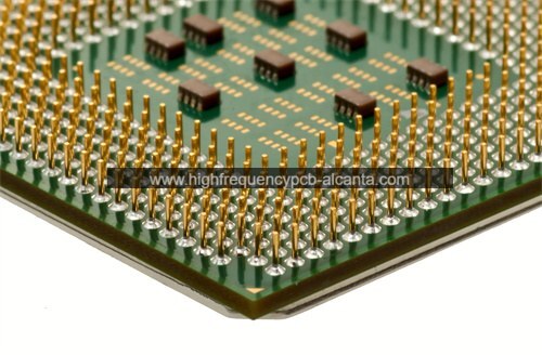
CSP Package Substrate
What are the functions of CSP Package Substrate?
The functions of CSP Package Substrate include:
Electrical connections: The CSP package substrate provides the crucial function of establishing electrical connections between the chip and the circuit board. It transmits electrical signals and power by connecting the pins or solder balls on the chip to corresponding connection points on the circuit board.
Mechanical support: In addition to electrical connections, the package substrate offers mechanical support for the chip. This helps protect the chip from mechanical stress and external environmental factors, ensuring stability during operation.
Thermal management: The CSP package substrate is also responsible for managing the heat generated by the chip. Through appropriate material selection and design, the substrate efficiently transfers heat from the chip to the surrounding environment, ensuring that the chip operates within the proper temperature range and avoiding damage due to overheating.
Signal transmission and noise suppression: The substrate plays a critical role in signal transmission, ensuring stable signal transfer and suppressing potential noise and interference.
Environmental protection: The substrate can also provide environmental protection for the chip, preventing damage from dust, moisture, and other external factors.
In summary, the CSP package substrate plays a key role by providing electrical connections and mechanical support, as well as managing heat, signal transmission, and environmental protection, ensuring the stable operation and long-term reliability of integrated circuits.
What are the different types of CSP Package Substrate?
There are several types of CSP package substrates, each designed to meet specific requirements and applications. Some common types include:
Organic Substrates: These substrates are made of organic materials such as epoxy resin or polyimide. They are lightweight, cost-effective, and offer good electrical performance. Organic substrates are commonly used in consumer electronics and mobile devices.
Ceramic Substrates: Ceramic substrates are made of materials like alumina or aluminum nitride. They offer excellent thermal conductivity and mechanical strength, making them suitable for high-power applications and environments where heat dissipation is critical.
Flexible Substrates: Flexible substrates are made of materials like polyimide or polyester. They are bendable and conformable, making them ideal for applications where flexibility is required, such as wearable electronics or curved displays.
Metal Substrates: Metal substrates are typically made of materials like copper or aluminum. They offer superior thermal conductivity and mechanical strength compared to organic substrates, making them suitable for high-power and high-frequency applications.
Glass Substrates: Glass substrates provide excellent dimensional stability and electrical insulation. They are often used in applications requiring high precision and reliability, such as medical devices or automotive electronics.
Composite Substrates: Composite substrates combine different materials to achieve specific properties, such as enhanced thermal performance or reduced weight. They are used in various applications depending on the desired characteristics.
These are just a few examples of CSP package substrates, and new types may emerge as technology advances and new requirements arise in the electronics industry.
What is the relationship between CSP Package Substrate and IC packaging?
CSP Package Substrate and IC (Integrated Circuit) packaging are closely related components in the assembly and protection of integrated circuits. Here’s how they are connected:
IC Packaging Incorporates CSP Technology: CSP (Chip Scale Package) is a type of IC packaging technology where the package is designed to be nearly the same size as the silicon die within it. CSP packaging integrates the substrate, connections, and protective casing into a compact form directly around the chip. Therefore, the CSP package substrate is an integral part of CSP IC packaging.
Substrate Provides Electrical Connections: The package substrate serves as the medium for establishing electrical connections between the integrated circuit (IC) chip and the external circuitry or system. It contains conductive traces or pads that connect the IC’s bond pads to the package’s external leads or solder balls, allowing for signal transmission and power distribution.
Mechanical Support and Protection: Both IC packaging and CSP package substrates provide mechanical support and protection to the delicate silicon die (chip). The substrate ensures that the chip is securely mounted within the package, protecting it from physical damage due to handling, environmental factors, or mechanical stresses during operation.
Thermal Management: Efficient heat dissipation is critical for the reliable operation of integrated circuits. IC packaging, including CSP technology, incorporates features for thermal management, such as heat sinks, thermal vias, or exposed pads. The package substrate plays a role in facilitating heat transfer away from the chip to the surrounding environment, ensuring proper thermal performance.
In summary, CSP Package Substrate is an essential component within IC packaging, providing electrical connections, mechanical support, and thermal management for the integrated circuit. The relationship between the two lies in their collaborative function to encapsulate and protect the chip while facilitating its connectivity and performance within electronic systems.
How does CSP Package Substrate differ from PCB?
CSP Package Substrate and PCB (Printed Circuit Board) are both essential components in electronic systems, but they serve different purposes and have distinct characteristics. Here are the key differences between them:
Function and Placement:
CSP Package Substrate: It serves as the foundation for mounting and connecting the integrated circuit (IC) chip directly. It provides electrical connections, mechanical support, and thermal management for the chip.
PCB: It acts as a platform for mounting various electronic components, including ICs, resistors, capacitors, and connectors. PCBs provide interconnections between these components and serve as the backbone of the electronic system.
Size and Form Factor:
CSP Package Substrate: It is typically much smaller in size, closely matching the dimensions of the IC chip it supports. CSPs are designed to minimize the package footprint, making them suitable for space-constrained applications.
PCB: PCBs can vary significantly in size and shape, depending on the complexity of the electronic system they support. They can range from small, single-layer boards to large, multi-layer boards used in complex devices like computers or industrial equipment.
Material and Construction:
CSP Package Substrate: Substrates for CSP packaging are often made of materials optimized for their electrical, thermal, and mechanical properties. Common materials include organic substrates (epoxy resin, polyimide), ceramics (alumina, aluminum nitride), or flexible materials (polyimide, polyester).
PCB: PCBs are typically made of fiberglass-reinforced epoxy laminates (FR-4), which provide good electrical insulation and mechanical strength. They consist of multiple layers of conductive traces separated by insulating layers, with components mounted on the surface or embedded within the layers.
Application and Integration:
CSP Package Substrate: CSP packaging is commonly used for mounting IC chips in compact electronic devices, such as mobile phones, tablets, and wearable devices, where space is limited, and high-density packaging is required.
PCB: PCBs are used in a wide range of electronic devices and systems, from consumer electronics to industrial machinery and aerospace applications. They provide a platform for integrating and interconnecting various electronic components to create functional systems.
In summary, while both CSP Package Substrate and PCB are integral to electronic systems, they differ in function, size, material, and application. CSP Package Substrate is specifically designed for mounting and connecting IC chips, whereas PCB serves as a platform for integrating and interconnecting electronic components in larger systems.
What are the structure and production technology of CSP Package Substrate?
The structure and production technology of CSP (Chip Scale Package) Package Substrate can vary depending on the specific materials and design requirements. However, I’ll provide a general overview of the typical structure and production process:
Structure:
Base Material: The substrate starts with a base material, which can be organic (e.g., epoxy resin, polyimide), ceramic (e.g., alumina, aluminum nitride), metal (e.g., copper), or composite material (e.g., fiberglass-reinforced epoxy laminates).
Conductive Layers: The substrate usually contains conductive layers made of copper or other metals. These layers provide the electrical pathways for connecting the IC chip to external circuitry.
Insulating Layers: Insulating layers separate the conductive layers to prevent short circuits. They are typically made of non-conductive materials such as resin or ceramic.
Via Holes: Via holes are small holes drilled or etched through the substrate to allow vertical electrical connections between different layers. These via holes can be filled with conductive material to establish electrical connections.
Surface Finish: The surface of the substrate may have a finish applied to enhance solderability and protect against corrosion. Common surface finishes include electroless nickel immersion gold (ENIG), hot air solder leveling (HASL), or organic surface protectant (OSP).
Production Technology:
Substrate Fabrication: The production process begins with the fabrication of the substrate material. For organic substrates, this involves laminating layers of resin and copper foil, followed by etching to define the circuit patterns. Ceramic substrates are formed through processes like casting, pressing, or firing.
Circuit Patterning: Conductive patterns are created on the substrate using techniques like photolithography, etching, or printing. This forms the traces, pads, and other electrical features required for chip mounting and interconnection.
Via Formation: Via holes are drilled or etched through the substrate using laser drilling, mechanical drilling, or chemical etching processes. These vias are then filled with conductive material to establish electrical connections between layers.
Surface Finish: After circuit patterning and via formation, the substrate may undergo surface finishing processes to improve solderability and protect against oxidation.
Assembly: Once the substrate is fabricated and finished, it is ready for IC chip attachment. This can involve processes such as soldering, wire bonding, or flip-chip bonding, depending on the specific packaging technology used.
Overall, the production of CSP Package Substrate involves a combination of material processing, circuit patterning, via formation, surface finishing, and assembly techniques to create a compact, reliable platform for mounting and connecting IC chips.
Frequently Asked Questions (FAQs):
What is CSP Package Substrate?
CSP Package Substrate refers to the material upon which the integrated circuit (IC) chip is mounted within a Chip Scale Package (CSP). It provides electrical connections, mechanical support, and thermal management for the chip.
What are the functions of CSP Package Substrate?
CSP Package Substrate performs several key functions, including providing electrical connections between the chip and external circuitry, offering mechanical support to the chip, managing heat dissipation, facilitating signal transmission, and protecting the chip from environmental factors.
What are the different types of CSP Package Substrate?
CSP Package Substrate can be made from various materials such as organic substrates (e.g., epoxy resin, polyimide), ceramic substrates (e.g., alumina, aluminum nitride), flexible substrates (e.g., polyimide, polyester), metal substrates (e.g., copper, aluminum), glass substrates, and composite substrates.
How does CSP Package Substrate differ from PCB?
While both CSP Package Substrate and Printed Circuit Board (PCB) are essential components in electronic systems, they serve different purposes. CSP Package Substrate is specifically designed for mounting and connecting IC chips, whereas PCB serves as a platform for integrating and interconnecting various electronic components in larger systems.
What is the relationship between CSP Package Substrate and IC packaging?
CSP Package Substrate is an integral part of IC packaging, providing electrical connections, mechanical support, thermal management, and other functionalities essential for encapsulating and protecting the integrated circuit (IC) chip within the package.
What is the structure and production technology of CSP Package Substrate?
The structure of CSP Package Substrate typically includes base material, conductive layers, insulating layers, via holes, and surface finish. The production technology involves substrate fabrication, circuit patterning, via formation, surface finishing, and assembly processes.
Conclusion
In conclusion, CSP Package Substrate is a crucial component in electronic systems, providing essential functions such as electrical connections, mechanical support, thermal management, and signal transmission for integrated circuit (IC) chips. It plays a pivotal role in IC packaging, contributing to the miniaturization, reliability, and performance of electronic devices.
CSP Package Substrate comes in various types, including organic, ceramic, flexible, metal, glass, and composite substrates, each tailored to meet specific requirements and applications. Its structure typically includes base material, conductive and insulating layers, via holes, and surface finish, fabricated through a series of production processes such as substrate fabrication, circuit patterning, via formation, surface finishing, and assembly.
Understanding the functions, types, and production technology of CSP Package Substrate is essential for designing and manufacturing advanced electronic systems with optimized performance and reliability. As technology continues to evolve, the role of CSP Package Substrate will remain pivotal in enabling innovative and efficient electronic devices for diverse applications.