 Professional high frequency circuit board supplier
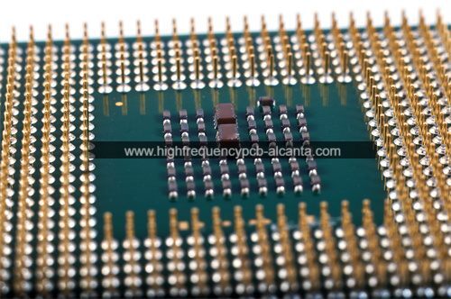
What is Ceramic Package Substrate?
Ceramic Package Substrate Supplier,Ceramic package substrate is a high-performance material widely used in semiconductor packaging for its excellent electrical properties and reliability. With superior thermal conductivity and mechanical strength, it ensures stable operation in demanding environments. Ceramic substrates offer low dielectric constants and minimal signal loss, making them ideal for high-frequency applications such as RF and microwave circuits. Commonly used in aerospace, automotive, and telecommunications industries, ceramic package substrates provide efficient heat dissipation and robust protection for semiconductor devices. Their precise construction and durability enable the development of compact and reliable electronic assemblies for various applications requiring high performance and longevity.
Let’s take a stroll through the realm of Ceramic Package Substrates—a specialized packaging wonder for our semiconductor friends. Picture it as the architectural maestro, setting the stage for the grand assembly of electronic virtuosos like integrated circuits (ICs), resistors, and capacitors. Crafted from the likes of ceramic artisans such as aluminum oxide (Al2O3) or aluminum nitride (AlN), this substrate boasts a prowess in thermal wizardry and mechanical fortitude.
In the face-off with the traditional printed circuit boards (PCBs), our ceramic maestro emerges victorious, donning a cape of advantages. Behold the enhanced thermal dance, the electrifying performance at frequencies that make heads spin, the reinforced mechanical backbone, and the stoic resistance to environmental mood swings—humidity and temperature variations beware!
In the grand design gallery, each Ceramic Package Substrate dons a unique attire, tailored to the semiconductor device’s desires and its destined adventures. Layers of ceramic elegance host secret metal pathways, conducting the symphony of electronic connections. Applauded on stages spanning telecommunications, automotive marvels, aerospace odysseys, and the kingdom of consumer electronics, these substrates take a bow as heroes in the tale of high-performance electronics.
Ceramic Package Substrate Supplier
What are the functions of Ceramic Package Substrate?
Enter the Ceramic Package Substrate, the silent powerhouse in the semiconductor arena, executing a multitude of pivotal functions:
Architectural Pillar: Envision it as the robust stage where electronic luminaries—integrated circuits (ICs), resistors, and capacitors—take center stage. Its mechanical support is the unsung hero, ensuring the semiconductor device stands tall.
Electric Choreographer: Deep within its composition lie concealed metal traces, orchestrating an intricate ballet of electrical connections among diverse components. It assumes the role of the conductor, harmonizing the flow of electrical signals with finesse.
Heat Conductor: Forged from ceramics boasting superior thermal conductivity, this substrate assumes the role of a conductor in the heat symphony, ensuring a graceful dissipation of heat generated by the electronic performers. No overheating theatrics allowed; it maintains a cool, composed ambiance.
Electrical Diplomat: Serving as an electrical insulator, the ceramic material diplomatically prevents unintended electrical dialogues among various components on the substrate. It’s akin to a mediator, preserving order in the electrical domain.
Weather-Resistant Guardian: In contrast to its organic counterparts, the ceramic substrate stands resilient against environmental adversaries. It bravely faces moisture, humidity, and temperature variations, acting as a protective guardian for the semiconductor device.
High-Frequency Virtuoso: Thanks to the distinctive properties of ceramics, these substrates shine in high-frequency performances. They contribute to the device’s ability to navigate swift signal processing, emerging as virtuosos in the dynamic realm of electronics.
Space-Saving Alchemist: In the era of compact elegance, ceramic packages demonstrate alchemical prowess in crafting miniaturized semiconductor devices. They play the role of space-saving alchemists, enabling sleek and efficient electronic designs.
In essence, the Ceramic Package Substrate emerges as the versatile virtuoso, seamlessly providing structural support, electrical connectivity, thermal finesse, environmental resilience, and high-frequency capabilities—a silent symphony conductor in the intricate play of semiconductor devices.
What are the different types of Ceramic Package Substrate?
Embark on a journey through the varied landscape of Ceramic Package Substrates, each crafted with a specific mission. Here’s a glimpse into the eclectic ensemble:
Multilayer Mosaic (LTCC/HTCC):
Low-Temperature Co-Fired Ceramic (LTCC): Unveiling intricate patterns at lower temperatures, LTCC substrates take center stage for complex designs.
High-Temperature Co-Fired Ceramic (HTCC): Ascending to higher temperatures, HTCC substrates emerge as the stalwarts, offering resilience for high-power and high-frequency escapades.
Thick Film Tapestry:
Thick film technology unveils a canvas of possibilities, involving the artful printing and firing of ceramic layers. These substrates shine in the realm of hybrid circuits and power electronics.
Thin Film Ballet:
Thin film technology delicately pirouettes on ceramic substrates, a perfect performance for applications demanding precision, like the intricate dance of microwave circuits.
Aluminum Nitride (AlN) Ballet:
AlN substrates, celebrated for their thermal grace, take the lead in the performance when efficient heat dissipation steals the spotlight. They often play a key role in high-power electronic productions.
Direct Bonded Copper (DBC) Sonata:
DBC substrates create a harmonious duet, blending ceramic (usually aluminum oxide) and directly bonded copper layers. This design, akin to a musical composition, offers stellar thermal conductivity and frequently finds a stage in power modules.
Ceramic Ball Grid Array (CBGA) Rhapsody:
CBGA packages perform an intricate symphony on ceramic substrates, adorned with a solder ball array for electrical connections. They often grace the stages of high-performance microprocessors and complex integrated circuits.
Chip-on-Board (COB) Minuet:
COB configurations showcase a minimalist dance, where semiconductor chips take the limelight directly on a ceramic substrate, bypassing the traditional packaging. It’s a performance tailored for those who appreciate the elegance of miniaturization and thermal efficiency.
Ceramic Dual In-Line Package (CerDIP) Overture:
CerDIP adds a ceramic twist to the classic Dual In-Line Package (DIP), presenting a timeless overture for the through-hole mounting of ICs.
Choosing the right Ceramic Package Substrate is akin to selecting the perfect piece for an orchestral composition—a decision influenced by thermal nuances, electrical harmonies, the pursuit of miniaturization, and the unique requirements of the electronic device or application. Each type contributes its unique notes to the symphony of possibilities in semiconductor packaging.
What is the relationship between Ceramic Package Substrate and IC packaging?
Imagine the synergy between Ceramic Package Substrates and IC packaging as an intricate dance routine, where each partner brings its unique flair to the semiconductor stage.
The Ceramic Package Substrate takes the lead, serving as the sturdy dance floor for the sophisticated moves of Integrated Circuits (ICs). It’s not just a passive surface but an active participant, providing structural support, electrical pathways, and a cool ambiance for the semiconductor performers to showcase their brilliance.
Now, enter IC packaging as the wardrobe designer of this electronic ballet. It’s the custom-made outfit that not only shields the IC but also ensures its graceful interaction with the external world. The packaging acts as a protective shield and a diplomatic envoy, enabling the IC to elegantly communicate with the broader electronic ensemble.
Together, Ceramic Package Substrates and IC packaging engage in a synchronized performance. The substrate establishes the groundwork, offering stability and thermal efficiency, while the packaging wraps the IC in a secure embrace, facilitating its seamless integration into the electronic choreography.
This collaboration is more than just a dance; it’s a strategic partnership crucial for achieving optimal performance, reliability, and functionality in semiconductor devices. The selection of Ceramic Package Substrate and IC packaging design becomes a carefully choreographed routine tailored to the specific application, thermal requirements, electrical nuances, and the pursuit of miniaturization. It’s a dynamic duet where each partner plays a distinct role, contributing to the flawless and efficient operation of the semiconductor device.
How does Ceramic Package Substrate differ from PCB?
Let’s unravel the distinct narratives of Ceramic Package Substrates and Printed Circuit Boards (PCBs), each contributing its own melody to the symphony of electronic design:
Material Marvels:
Ceramic Package Substrate: Sculpted from ceramic materials like aluminum oxide or aluminum nitride, exuding excellence in thermal conductivity and mechanical robustness.
PCB: Takes center stage with layers of fiberglass-reinforced epoxy, engaging in a dance with copper traces to weave electrical connections.
Applications Tapestry:
Ceramic Package Substrate: Assumes a leading role in high-performance domains such as microprocessors, where the spotlight is on thermal management and durability.
PCB: Dances through diverse electronic landscapes, seamlessly connecting components and showcasing its versatility in signal routing.
Thermal Ballet:
Ceramic Package Substrate: Dazzles with stellar thermal conductivity, a virtuoso in dissipating heat, particularly in the high-powered electronic arenas.
PCB: Executes its routine with reliable, though less extravagant, thermal conductivity, suited for applications with moderate thermal demands.
Strength Sonata:
Ceramic Package Substrate: Leads with a crescendo of mechanical strength, portraying resilience and resistance to mechanical stresses, making it a protagonist in durability-driven applications.
PCB: Contributes a reliable harmony of mechanical strength, performing capably across various scenarios but without the same durability finesse as ceramic substrates.
Cost Choreography:
Ceramic Package Substrate: Commands a higher ticket price, attributing its cost to the use of sophisticated ceramic materials and intricate manufacturing processes.
PCB: Executes a cost-effective routine, making it the preferred dancer in productions where versatility and budget considerations take the lead.
In the grand theater of electronics, the choice between Ceramic Package Substrates and PCBs depends on the specific act being orchestrated. The former claims the spotlight for its thermal prowess and durability, while the latter gracefully pirouettes through a diverse array of electronic productions, embodying versatility and cost-effectiveness.
What are the structure and production technology of Ceramic Package Substrate?
Embark on a journey into the intricate world of Ceramic Package Substrate, where both structure and production technology unfold like chapters in a fascinating tale:
Structure:
Foundational Ceramics:
The narrative begins with ceramics, often starring aluminum oxide (Al2O3) or aluminum nitride (AlN), chosen for their stellar thermal conductivity and mechanical prowess.
Layered Symphony:
Multiple layers weave a tapestry, each layer contributing a unique element – be it electrical pathways, mechanical reinforcement, or insulation.
Metallic Trails:
Within the ceramic labyrinth, metallic trails meander, forming an intricate network for electrical connectivity between components.
Insulating Overture:
Dielectric layers take center stage, ensuring a harmonious separation of conductive trails to avoid unintended electronic crosstalk.
Metallurgical Ballet:
Certain areas undergo a metamorphic process, donning metallization to enhance conductivity and establish a graceful bond with electronic companions.
Solder Mask Veil:
A delicate solder mask is applied, akin to a protective veil, shielding the conductive traces and preventing inadvertent soldering during the assembly ball.
Production Technology:
Ceramic Alchemy:
Raw ceramic materials undergo a transformative alchemy, transitioning from powders to structured forms through meticulous mixing, milling, and shaping.
LTCC Tapestry (for LTCC):
In the enchanting Low-Temperature Co-Fired Ceramic (LTCC) tapestry, ceramic material is woven into “green tapes,” laying the foundation for multilayer creations.
HTCC Canvas (for HTCC):
High-Temperature Co-Fired Ceramic (HTCC) takes the stage with layers painted onto the canvas, undergoing a fiery ordeal to achieve the desired density and form.
Sintering Saga:
The characters, be it green tapes or painted layers, engage in a transformative sintering saga, subjected to intense heat to solidify their roles in the ceramic narrative.
Metallic Elegance:
Conductive metals make a grand entrance, depositing themselves onto the ceramic canvas through the artistry of thin-film deposition or the precision of thick-film printing.
Patterning Ballet:
Patterning techniques like photolithography choreograph a dance of circuit patterns, defining the intricate steps each component will take on the substrate stage.
Assembling Crescendo:
The grand finale unfolds as electronic components, the stars of the show, take their places on the substrate stage through various assembly techniques.
Quality Control Symphony:
The finished substrate undergoes a meticulous quality control symphony, where electrical connectivity, thermal performance, and overall reliability are assessed with a critical ear.
The tale of Ceramic Package Substrate is not just a technological account; it’s a narrative rich in characters, layers, and transformative processes, where each element contributes to the seamless performance of electronic devices.
Frequently Asked Questions (FAQs)
Where does the influence of Ceramic Package Substrates extend?
The impact reverberates across electronic devices, gracing microprocessors, memory modules, power amplifiers, and high-frequency circuits. Their selection is a delicate dance, choreographed by their adeptness in thermal management and unwavering reliability.
What virtues do Ceramic Package Substrates bring to the stage?
These substrates boast an ensemble of virtues—high thermal conductivity, impeccable mechanical strength, and unwavering reliability. They take center stage in applications demanding an exquisite blend of efficient heat dissipation, durability, and steadfast stability.
What role does Ceramic Package Substrate play in the realm of thermal management?
Armed with high thermal conductivity, ceramic substrates elegantly dissipate the heat choreographed by electronic components. This characteristic is especially critical in high-powered performances, ensuring a symphony of optimal device performance and enduring longevity.
How is the choice orchestrated between different Ceramic Package Substrate types?
Selection becomes a meticulous dance, orchestrated by specific application needs—thermal requirements, electrical characteristics, mechanical fortitude, and the desired miniaturization levels. LTCC, HTCC, AlN, and DBC each emerge as protagonists, offering unique advantages for diverse scenarios.
Can Ceramic Package Substrates take the spotlight in high-frequency performances?
Indeed, certain types, such as LTCC, showcase their prowess in high-frequency performances. Their design and material properties harmonize seamlessly with the demands of circuits dancing to elevated frequencies.
How do the verses of Ceramic Package Substrates differ from organic substrates like FR-4 PCBs?
In the grand composition, Ceramic Package Substrates, leveraging materials like aluminum oxide or aluminum nitride, transcend the verses of organic substrates like FR-4 PCBs. They emerge as the virtuosos, particularly in applications with stringent thermal prerequisites.
Are there environmental considerations in the Ceramic Package Substrate’s composition?
The ceramic ensemble generally exhibits a greener note. Their durability and resilience to harsh conditions contribute a sustainable cadence to the longevity and reliability of electronic devices.
Conclusion
In closing, Ceramic Package Substrates emerge as silent architects in the intricate ballet of electronic packaging, providing a sturdy canvas for the integration and performance of integrated circuits (ICs). Forged from ceramics like aluminum oxide or aluminum nitride, these substrates unveil a saga of exceptional thermal conductivity and mechanical fortitude, becoming linchpins in applications that demand the delicate interplay of efficient heat dissipation and enduring durability.
With a diverse cast of types such as Low-Temperature Co-Fired Ceramic (LTCC), High-Temperature Co-Fired Ceramic (HTCC), Aluminum Nitride (AlN), and Direct Bonded Copper (DBC), Ceramic Package Substrates don various roles across the electronic stage. Their production narrative, painted with specialized strokes like LTCC or HTCC, diverges from the conventional script of Printed Circuit Boards (PCBs), carving out a distinctive niche in the evolving narrative of electronic design.
The virtues of high thermal conductivity, impeccable mechanical strength, and unwavering reliability form the melodic undertones of Ceramic Package Substrates in the electronic symphony. From the nuanced pirouettes of microprocessors and memory modules to the commanding crescendos of power amplifiers and high-frequency circuits, these substrates not only elevate performance but also lay the groundwork for stability and endurance in challenging environments.
Ceramic Package Substrates, akin to conductors in a grand orchestral piece, masterfully manage the thermal landscape. Their proficiency in efficiently dissipating heat not only ensures the optimal resonance of device performance but also orchestrates a lasting ode to the endurance and longevity of the electronic composition. The selection process unfolds as a choreography of considerations, where different substrate types execute tailored performances to meet the nuanced needs of diverse applications.
In the vast composition of electronic design, Ceramic Package Substrates emerge as virtuosos, not merely for their technical prowess but also for their harmonious integration with environmental sustainability. Their robust composition and resilience to the rigors of environmental elements compose a rhythmic cadence, contributing to the longevity and reliability of electronic devices, seamlessly weaving into the electronic ensemble.
In essence, the story of Ceramic Package Substrates is a narrative of innovation and resilience, etching its imprint on the canvas of electronic design and enriching the performance and reliability of electronic systems. As these substrates take their bow on the stage, their contribution extends beyond the realm of material properties, becoming an integral part of the evolving sonnet of modern electronic devices.