 Professional high frequency circuit board supplier
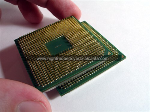
What is Cavity Package Substrate?
Cavity Package Substrate Manufacturer,Cavity package substrate is a specialized material designed for housing and protecting sensitive electronic components. It features a recessed cavity that accommodates chips and other devices, providing robust mechanical support and enhanced thermal management. This design minimizes thermal and mechanical stresses on the components, ensuring reliable performance in high-frequency and high-power applications. Cavity package substrates offer low dielectric constants and minimal signal loss, ideal for RF and microwave circuits. Widely used in aerospace, military, and telecommunications industries, they enable compact and efficient electronic assemblies with superior signal integrity and durability.
Cavity Package Substrate (CPS) stands out as a pioneering packaging solution within the realm of semiconductor devices, aiming to revolutionize the integration of integrated circuits (ICs) or chips. The hallmark of this innovative technology lies in its creation of a void or cavity within the substrate, strategically tailored to securely house the chip.
At its core, CPS technology pursues a dual objective: the reduction of overall package size while concurrently enhancing or at least maintaining the semiconductor device’s performance. This paradigm shift is particularly instrumental in applications where spatial constraints and weight considerations take center stage, such as the development of portable electronic gadgets, including mobile devices and wearables.
Several distinctive characteristics define the Cavity Package Substrate:
Compactness Redefined: CPS substrates usher in a departure from conventional packaging norms, ushering in a reduction in package dimensions. This departure is pivotal in sculpting smaller and sleeker electronic devices.
Thermal Wizardry: The cavity design of CPS doesn’t just cater to aesthetics; it actively facilitates superior heat dissipation from the chip. This functionality acts as a thermal guardian, averting overheating issues and ensuring the semiconductor device operates within optimal temperature thresholds.
Electrical Alchemy: Beyond its physical structure, the substrate’s design nuances contribute to an augmented electrical performance. This translates into minimized parasitic capacitance and inductance, nurturing an environment conducive to robust signal integrity.
Weight Watchers’ Delight: Shedding excess material, CPS substrates actively partake in a weight reduction spree. This attribute holds particular significance in handheld devices like mobile phones, contributing to a more lightweight and manageable user experience.
Economic Packaging Poetry: CPS substrates, with their streamlined design and reduced material requirements, compose an economic ode in the manufacturing symphony. The resulting cost-effectiveness adds a practical dimension to their appeal.
In a tech landscape gravitating towards smaller yet mightier electronic marvels, CPS technology has garnered widespread acclaim. However, its implementation requires a nuanced approach, carefully navigating the intricate dance between miniaturization benefits and the imperative for durable, resilient semiconductor devices.
Cavity Package Substrate Manufacturer
What is the Function of Cavity Package Substrate?
Cavity Package Substrate (CPS) serves as a linchpin in the intricate dance of semiconductor innovation, orchestrating an ensemble of functions that redefine the landscape of integrated circuits. Let’s unravel the tapestry of CPS functions:
Architectural Alchemy: At its core, CPS is a maestro of architectural ingenuity. It ingeniously carves out a void within the substrate, creating a bespoke accommodation for the chip. This architectural alchemy lays the foundation for a paradigm shift towards more compact and seamlessly integrated semiconductor devices.
Thermal Symphony Conductor: Beyond its aesthetic appeal, CPS steps into the role of a symphony conductor for thermal dynamics. The crafted cavity emerges as a conduit for the graceful dissipation of heat from the chip. This isn’t just about preventing overheating; it’s about orchestrating an environment where the semiconductor device performs in harmony within its optimal temperature range.
Electrical Ballet: CPS takes center stage in an electrical ballet, where every move is deliberate. The substrate’s design intricacies, including the reduction of parasitic capacitance and inductance, choreograph an environment conducive to the graceful dance of electrical signals. This choreography is pivotal for maintaining the integrity and reliability of semiconductor devices.
Weightless Waltz Partner: Shedding excess baggage, CPS engages in a weightless waltz, contributing to the allure of lighter electronic devices. Stripping away unnecessary material, it becomes a valued partner in the quest for a more ergonomic and portable user experience, especially in the realm of handheld gadgets.
Economic Artisan: CPS transforms into an economic artisan, sculpting a packaging solution that is not just technologically advanced but also economically astute. Its streamlined design and efficient material usage become strokes of economic artistry, resulting in a cost-effective solution for manufacturing electronic devices.
Guardian of Reliability: Beyond its technical prowess, the CPS-crafted cavity assumes the role of a guardian, sheltering the semiconductor device from the caprices of the external environment. This protective embrace enhances the durability and reliability of the packaged component, ensuring it weathers the challenges of real-world usage.
In essence, the function of Cavity Package Substrate is a harmonious composition of architectural brilliance, thermal finesse, electrical precision, weight-conscious partnering, economic astuteness, and reliability guardianship. As the realm of electronic devices evolves, CPS stands poised as a virtuoso, addressing the call for smaller, more efficient, and dependable semiconductor solutions.
What Are the Different Types of Cavity Package Substrate?
Cavity Package Substrates (CPS) exhibit a diverse array of incarnations, each meticulously tailored to fulfill distinct roles across various applications and performance criteria. Let’s delve into the assortment of CPS types:
Ceramic Ensemble:
Composition: Fashioned from ceramic materials like alumina or aluminum nitride.
Attributes: Ceramic substrates, with their commendable thermal conductivity, take center stage in applications where efficient heat dissipation is non-negotiable.
Organic Odyssey:
Composition: Embraces organic materials, often epoxy-based, to form the substrate.
Attributes: Organic substrates carve a niche as cost-effective and lightweight alternatives, finding resonance in applications where thermal considerations play a supporting role.
Metallic Melody:
Composition: Weaves metals such as copper or aluminum into the substrate fabric.
Attributes: Metal substrates, with their symphony of thermal conductivity and mechanical robustness, strike a chord in applications demanding both thermal resilience and structural fortitude.
Flex-Finesse:
Composition: Exploits flexible materials like polyimide or liquid crystal polymer (LCP).
Attributes: Flexible substrates choreograph a dance of adaptability, catering to the needs of applications seeking flexibility and contortion capability.
Stratified Sonata:
Structure: Unfurls as a layered composition, stacking multiple substrate strata.
Attributes: Multi-layer substrates compose a harmonious symphony for intricate circuit designs, enabling higher integration levels for electronic devices nestled in tight spatial confines.
Glass Serenade:
Composition: Incorporates glass into the substrate repertoire.
Attributes: Glass substrates hit the right notes with high thermal stability, presenting an ideal canvas for applications demanding packaging solutions with enduring reliability.
LTCC Crescendo:
Composition: Embraces Low-Temperature Co-Fired Ceramic (LTCC) as a substrate medium.
Attributes: LTCC substrates crescendo into the spotlight with stellar electrical performance, harmonizing with low firing temperatures to accommodate temperature-sensitive components.
RF Harmonics:
Application: Tailored exclusively for RF and microwave applications.
Attributes: RF substrates orchestrate a symphony of minimized signal losses, attuning themselves to the demands of high-frequency scenarios.
HDI Rhapsody:
Structure: Incorporates the artistry of High-Density Interconnect (HDI) technology.
Attributes: HDI substrates compose a rhapsody of finer lines and spaces, conducting the design of compact and high-performance electronic devices.
The selection of a particular Cavity Package Substrate is akin to orchestrating a symphony, where manufacturers carefully choose the composition that resonates harmoniously with the unique demands of the semiconductor device and the overarching design vision.
What is the Relationship Between Cavity Package Substrate and IC Packaging?
The interplay between Cavity Package Substrate (CPS) and IC packaging is a dynamic partnership, where each element complements and enhances the objectives of the other within the intricate realm of integrated circuits (ICs). Let’s navigate the nuanced connection between CPS and IC packaging:
Precision of Placement:
CPS’s Role: CPS intricately carves out a designated space within its substrate to cradle the IC securely.
IC Packaging Harmony: This precision in spatial design aligns seamlessly with the core tenet of IC packaging – the encapsulation and protection of the IC within a robust exterior. CPS’s crafted cavity becomes the tailored enclosure, fostering a harmonious fit.
Thermal Synchrony:
CPS’s Role: Adept at dissipating heat efficiently, CPS leverages its designed cavity to facilitate heat dissipation from the IC.
IC Packaging Symbiosis: Thermal regulation is pivotal in IC packaging to prevent overheating. CPS’s thermal proficiency aligns cohesively with the broader packaging agenda, ensuring the IC maintains its optimal operating temperature.
Electrical Integration Ballet:
CPS’s Role: CPS optimizes electrical performance through meticulous design, minimizing parasitic capacitance and inductance.
IC Packaging Choreography: IC packaging is inherently concerned with preserving electrical integrity. CPS’s finesse in electrical considerations harmonizes with this goal, contributing to the overall dependability and performance of the packaged IC.
Form Factor Fusion:
CPS’s Role: Embracing diversity in its types, such as flexible or multi-layer substrates, CPS accommodates a spectrum of form factors.
IC Packaging Adaptation: Form factor considerations are pivotal in IC packaging, especially in the era of miniaturization. The flexibility and adaptability of CPS substrates contribute significantly to achieving diverse form factors for packaged ICs.
Material Collaboration:
CPS’s Role: CPS offers a range of material compositions, from ceramic to organic or metal, each with distinct properties.
IC Packaging Synergy: The choice of packaging materials is a decisive factor in IC packaging. CPS’s material options provide a palette for customization, allowing for substrates that align precisely with the unique needs of the IC and its intended application.
Economical Ensemble:
CPS’s Role: With its streamlined design, CPS contributes to cost efficiency in the manufacturing process.
IC Packaging Efficiency: Cost-effectiveness is a paramount consideration in IC packaging. CPS’s economic advantages resonate with the overarching goal of achieving efficient and budget-friendly packaging solutions for ICs.
In essence, the liaison between Cavity Package Substrate and IC packaging is a synergistic dance, where CPS serves as a specialized foundation, enhancing and harmonizing with the broader objectives of IC packaging. From spatial accommodation to thermal equilibrium, electrical integrity, form factor flexibility, material synergy, and economic efficiency, each element plays a unique yet interwoven role in the packaging symphony of integrated circuits.
How Does Cavity Package Substrate Differ from Regular PCBs?
Cavity Package Substrates (CPS) and traditional Printed Circuit Boards (PCBs) navigate divergent paths in the electronic landscape, each sculpted to address specific demands. Let’s delve into the facets that set them apart:
Cavity-Centric Craftsmanship:
CPS: Distinguished by its intentional carving of a cavity within the substrate, creating a tailored shelter for semiconductor devices like integrated circuits (ICs) or chips.
Regular PCBs: In contrast, regular PCBs unfold on a flat canvas, offering a versatile terrain for an array of electronic components without the specialized alcove for individual chips.
Application Essence:
CPS: Crafted with a focal point on packaging and safeguarding semiconductor devices, placing emphasis on miniaturization, thermal equilibrium, and optimizing electrical performance.
Regular PCBs: Crafted as functional circuit arenas, prioritizing connectivity and overall functionality over the encapsulation and protection of specific chips.
Miniaturization Ballet:
CPS: Choreographs a dance of compact integration for chips, finding resonance in applications with spatial constraints, such as the realms of mobile devices and wearables.
Regular PCBs: Contributes to the symphony of functional circuits, without the intricate steps required for housing semiconductor devices in dedicated cavities.
Thermal Sonata:
CPS: Orchestrates a thermal symphony, specifically designed to ensure a graceful dissipation of heat from enclosed chips, maintaining a harmonious temperature balance.
Regular PCBs: Acknowledges the thermal considerations without the same resounding notes, adjusting priorities based on the broader thermal needs of the system.
Design Flexibility Waltz:
CPS: Steps into the realm of flexibility, incorporating materials that allow for adaptability in the substrate – a key performer in applications demanding the grace of bendable or flexible electronic devices.
Regular PCBs: Perform on a more rigid stage, primarily constructed with inflexible materials. For the dance of flexibility, flexible PCBs take the lead.
Material Palette Composition:
CPS: Weaves a tapestry using a diverse selection of materials – ceramics, metals, organics, or blends – attuned to the specific needs of thermal, electrical, and mechanical intricacies.
Regular PCBs: Paints with a more standardized palette, often relying on materials like FR-4 (an epoxy variant), capturing a balance between economical pragmatism and performance.
Economic Symphony:
CPS: Takes center stage with a specialized performance, potentially contributing to a higher production cost based on the choreography required for specific applications.
Regular PCBs: Operate on a more economically straightforward stage, leveraging standardized designs and materials to compose a cost-effective symphony.
In essence, Cavity Package Substrates and regular PCBs navigate unique roles in the electronic orchestration. CPS directs the spotlight towards encapsulating and protecting semiconductor devices with a nuanced focus on miniaturization and thermal mastery, while regular PCBs serve as versatile stages for diverse electronic components, emphasizing connectivity and functionality across various applications.
What are the Main Structures and Production Technologies of Cavity Package Substrate?
Cavity Package Substrates (CPS) boast diverse structures and production technologies, meticulously chosen to align with the intricate demands of semiconductor devices. Here’s an exploration of the primary structures and production methods associated with CPS:
Structures:
Single-Layer Symphony:
Overview: The fundamental CPS structure featuring a single substrate layer, ingeniously designed to incorporate a cavity for the accommodation of semiconductor devices.
Applications: Well-suited for less complex electronic applications where simplicity meets the requirements.
Harmonious Multi-Layer Ensemble:
Overview: An orchestration of multiple substrate layers stacked together, providing a symphony of increased routing density and support for intricate circuit designs.
Applications: Ideal for applications demanding complexity and a heightened level of integration.
Flex Melody:
Overview: Weaves flexibility into the substrate using materials like polyimide or liquid crystal polymer, allowing for a dynamic and adaptable structure.
Applications: Tailored for flexible and bendable electronic devices where rigidity takes a backseat.
HDI Crescendo:
Overview: Incorporates High-Density Interconnect (HDI) technology, conducting a refined composition with finer lines and spaces for heightened routing density.
Applications: Ideal for applications thirsty for increased circuit density and a reduction in spatial footprint.
Production Technologies:
Laser Artistry:
Description: Deploys laser precision to sculpt substrates, selectively removing material to craft cavities and intricate patterns.
Applications: A preferred technique for precise cavity creation and substrate detailing.
Chemical Etching Ballet:
Description: Engages chemical solutions to elegantly remove material selectively, crafting cavities and well-defined structures.
Applications: Frequently used in shaping substrates and creating intricate patterns.
Thin-Film Serenade:
Description: Deploys thin film deposition techniques to adorn the substrate with thin layers of materials, transforming its properties.
Applications: Enhances electrical conductivity, thermal characteristics, or introduces specific layers within the substrate.
Laminating Harmony:
Description: Bonds substrate layers with finesse using heat and pressure, achieving structural integrity and cohesion.
Applications: Commonly applied in the production of multi-layer CPS to enhance overall robustness.
Micro-Machining Sonata:
Description: Taps into precision machining techniques, such as micro-milling or micro-drilling, to sculpt small features and structures.
Applications: Ideal for crafting intricate details, perforations, or channels within the substrate.
Additive Manufacturing Overture (3D Printing):
Description: Constructs substrates layer by layer through additive processes, allowing for intricate and customizable designs.
Applications: An emerging frontier for crafting CPS with unique and tailored structures.
Screen Printing Composition:
Description: Applies conductive or dielectric materials through a mesh screen onto the substrate surface.
Applications: Effective for creating patterns, conductive traces, and insulating layers with a tactile precision.
These structures and production techniques serve as a diverse repertoire, allowing for nuanced customization and adaptability in the creation of Cavity Package Substrates to suit the intricate needs of semiconductor devices and applications.
Frequently Asked Questions (FAQs)
What Constitutes a Cavity Package Substrate (CPS)?
Cavity Package Substrate (CPS) stands out as a distinctive substrate used in semiconductor packaging. It features a purposeful cavity within its structure, serving as a designated housing for semiconductor devices like integrated circuits (ICs) or chips.
What Role Does the Cavity Play in CPS?
The cavity within CPS serves multifaceted functions. It provides a shielded enclosure for semiconductor devices, enhances thermal dissipation capabilities, and meets specific form factor requirements essential in various electronic applications.
In Which Applications Can CPS Be Found?
CPS finds utility in an array of electronic devices, particularly those with spatial limitations. Common applications encompass mobile devices, wearables, RF/microwave components, and any scenario where efficient thermal management and compact design are paramount.
What Are the Varied Structures of Cavity Package Substrates?
CPS structures can be singular or multi-layered, flexible, or incorporate High-Density Interconnect (HDI) technology. The selection depends on factors such as circuit complexity, integration needs, and flexibility requirements.
How Does CPS Differ from Conventional Printed Circuit Boards (PCBs)?
CPS is purpose-built for semiconductor packaging, featuring a dedicated cavity for chip accommodation and emphasizing thermal management. In contrast, regular PCBs are versatile and focus on providing a platform for electronic components without the specialized housing for semiconductor devices.
Can CPS Structures Be Tailored for Specific Applications?
Absolutely, CPS structures are customizable to align with the distinct requirements of semiconductor devices and applications. This includes variations in layer count, material selection, and the integration of flexible or rigid substrates.
Is CPS a Cost-Efficient Solution?
The cost of CPS can vary, influenced by factors such as material choices, structural complexity, and production technologies. While specialized designs may incur higher costs, the efficiency of CPS in thermal management and miniaturization often contributes to overall system cost-effectiveness.
Conclusion
In summary, Cavity Package Substrates (CPS) emerge as a sophisticated and adaptable solution in the intricate domain of semiconductor packaging. The deliberate incorporation of a cavity within the substrate not only shields semiconductor devices but also significantly contributes to effective thermal regulation and the pursuit of miniaturization. CPS structures exhibit a rich diversity, spanning from single-layer configurations to multi-layer orchestrations, flexible adaptations, and those incorporating cutting-edge technologies like High-Density Interconnect (HDI).
The selection of materials for CPS, spanning ceramics, metals, organics, and flexible compounds, underscores its versatility in meeting the dynamic requirements of electronic applications. This flexibility extends to the customization of CPS structures, offering a tailored approach to accommodate the specific needs of semiconductor devices and diverse applications characterized by varying spatial constraints.
The production technologies deployed in crafting CPS, including laser ablation, chemical etching, and additive manufacturing, showcase a blend of precision and innovation, laying the foundation for the creation of intricate structures that resonate with electronic designers.
CPS finds its niche in a broad spectrum of applications, ranging from mobile devices to wearables and RF/microwave components, underscoring its relevance in contemporary electronic landscapes. The designed cavity serves not only as a secure enclave for semiconductor devices but also as a catalyst for improved thermal dissipation, enhancing the overall reliability and performance of electronic systems.
While CPS may entail specific costs associated with its specialized design and materials, its efficacy in meeting thermal and miniaturization demands often translates into a judiciously cost-effective solution across diverse electronic applications.
In essence, Cavity Package Substrates strike a harmonious balance between functionality, adaptability, and precision, positioning themselves as integral players in the unfolding narrative of semiconductor packaging technologies. As electronic devices continue their progression, CPS stands ready to meet the challenges of evolving technologies, ensuring the resilience and efficiency of semiconductor components in a myriad of applications.