 Professional high frequency circuit board supplier
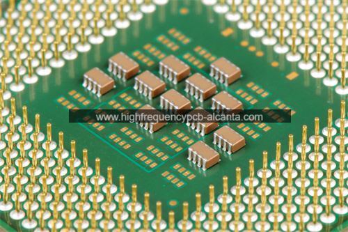
What is Ball Grid Array Package Substrate?
Ball Grid Array Package Substrate Manufacturer,Ball Grid Array (BGA) package substrate is a key component in semiconductor packaging, featuring a grid of solder balls on its underside for reliable electrical connections. BGA substrates support high-density integration of chips, minimizing footprint and enhancing performance. With advanced materials and precise manufacturing, they ensure efficient signal transmission and thermal management. Widely used in computing, telecommunications, and automotive industries, BGA package substrates facilitate compact and reliable electronic assemblies. Their robust construction and compatibility with various components make BGA substrates essential for developing cutting-edge electronic systems with superior performance and longevity.
A Ball Grid Array (BGA) package substrate is a type of integrated circuit packaging technology used in electronic devices. It’s a method of connecting an integrated circuit (IC) to a printed circuit board (PCB). The BGA package substrate consists of a thin layer of insulating material, typically made of fiberglass-reinforced epoxy resin, with copper traces and pads on its surface.
In a BGA package, instead of using traditional leads or pins, solder balls are used to make electrical connections between the IC and the PCB. These solder balls are arranged in a grid pattern on the underside of the package substrate, hence the name “Ball Grid Array.” The IC is mounted onto the substrate, and during assembly, the solder balls are heated, melting them and creating a connection between the IC and the PCB.
BGA packages offer several advantages over traditional packaging methods, including a higher density of connections, better electrical performance, and improved thermal management. These features make BGA packages suitable for a wide range of applications, including microprocessors, memory chips, and other high-performance integrated circuits in various electronic devices such as computers, smartphones, and networking equipment.
Ball Grid Array Package Substrate Manufacturer
What are the Functions of Ball Grid Array Package Substrate?
The Ball Grid Array (BGA) package substrate serves several important functions in electronic devices:
Electrical connections: The substrate provides a platform for connecting the integrated circuit (IC) to the printed circuit board (PCB). It contains conductive traces and pads that route signals between the IC and the PCB, facilitating the flow of electricity between components.
Mechanical support: The substrate offers structural support for the IC, helping to secure it in place on the PCB. This is particularly important in applications where the device may be subject to mechanical stress or vibration.
Thermal management: The substrate plays a role in dissipating heat generated by the IC during operation. By providing a path for heat to flow away from the IC and into the PCB, the substrate helps prevent overheating and ensures the reliable performance of the device.
Signal integrity: The design of the substrate, including the layout of the traces and pads, can impact the quality of electrical signals transmitted between the IC and the PCB. By optimizing signal paths and minimizing interference, the substrate helps maintain signal integrity and ensure the accurate transmission of data.
Package protection: The substrate acts as a protective barrier for the IC, shielding it from environmental factors such as moisture, dust, and mechanical damage. This helps prolong the lifespan of the IC and ensures its reliability in various operating conditions.
Overall, the BGA package substrate is a critical component in electronic devices, providing essential functions that contribute to the performance, reliability, and longevity of the device.
What are the Different Types of Ball Grid Array Package Substrate?
There are several different types of Ball Grid Array (BGA) package substrates, each with its own characteristics and intended applications. Some common types include:
Organic Substrates: These substrates are made of organic materials such as fiberglass-reinforced epoxy resin. They are lightweight, cost-effective, and widely used in consumer electronics, telecommunications, and computing devices.
Ceramic Substrates: Ceramic substrates are made of materials like alumina (aluminum oxide) or aluminum nitride. They offer excellent thermal conductivity, mechanical strength, and reliability, making them suitable for high-performance applications such as aerospace, automotive, and military electronics.
Flex Substrates: Flex substrates are flexible printed circuit boards (PCBs) made of materials like polyimide. They are used in applications where flexibility is required, such as wearable devices, automotive electronics, and medical devices.
Metal Substrates: Metal substrates, also known as metal-core PCBs, have a layer of metal (usually aluminum) as the base material. They offer excellent thermal conductivity and are commonly used in high-power LED lighting, automotive electronics, and power electronics.
Embedded Substrates: Embedded substrates incorporate additional components or features within the substrate itself, such as passive components (e.g., resistors, capacitors), embedded antennas, or sensors. They are used in applications where space-saving or integration of multiple functions is required.
Each type of BGA package substrate has its own advantages and limitations, and the choice depends on factors such as performance requirements, cost considerations, and specific application needs.
How does Ball Grid Array Package Substrate Relate to IC Packaging?
Ball Grid Array (BGA) package substrate is a crucial element in IC (Integrated Circuit) packaging. IC packaging involves enclosing the integrated circuit (IC) die within a protective housing or package, providing electrical connections, thermal management, and mechanical support. The BGA package substrate serves as the interface between the IC die and the printed circuit board (PCB) in the larger electronic system.
Here’s how BGA package substrate relates to IC packaging:
Electrical connections: BGA package substrate provides a platform for connecting the IC die to the PCB. It contains conductive traces and pads that facilitate electrical connections between the IC and the external circuitry on the PCB. This is essential for the transmission of signals between the IC and other components in the system.
Thermal management: BGA package substrate plays a crucial role in dissipating heat generated by the IC during operation. It provides a thermal path for heat to flow away from the IC and into the PCB, helping to prevent overheating and maintain the IC’s performance and reliability.
Mechanical support: The substrate offers structural support for the IC die, helping to secure it in place within the package and on the PCB. This is important for ensuring the mechanical integrity of the IC package, especially in applications where the device may be subject to mechanical stress or vibration.
Package protection: BGA package substrate acts as a protective barrier for the IC die, shielding it from environmental factors such as moisture, dust, and mechanical damage. This helps to prolong the lifespan of the IC and ensure its reliability in various operating conditions.
In summary, BGA package substrate is an integral part of IC packaging, providing essential functions such as electrical connections, thermal management, mechanical support, and package protection. It serves as the interface between the IC die and the larger electronic system, facilitating the reliable operation of integrated circuits in various applications.
What are the Differences Between Ball Grid Array Package Substrate and PCB?
Ball Grid Array (BGA) package substrate and Printed Circuit Board (PCB) are both essential components in electronic devices, but they serve different purposes and have distinct characteristics. Here are some key differences between them:
Function:
BGA package substrate: The primary function of a BGA package substrate is to provide a platform for connecting the integrated circuit (IC) to the printed circuit board (PCB). It facilitates electrical connections, thermal management, and mechanical support specifically for the IC.
PCB: A PCB serves as the foundation for mounting various electronic components and providing interconnections between them. It acts as a platform for assembling and connecting electronic circuits, including but not limited to ICs.
Construction:
BGA package substrate: The substrate used in BGA packages is typically a thin layer of insulating material (e.g., fiberglass-reinforced epoxy resin) with copper traces and pads on its surface. It may also include solder balls for connecting the IC to the PCB.
PCB: A PCB consists of multiple layers of insulating material (e.g., fiberglass or composite epoxy) with conductive traces etched onto them. These traces create electrical pathways between the various components mounted on the PCB.
Size and Complexity:
BGA package substrate: BGA substrates are generally smaller and less complex than PCBs. They are designed to accommodate a single integrated circuit and provide specific functions tailored to the IC’s requirements.
PCB: PCBs can vary significantly in size and complexity depending on the application. They can range from simple single-layer boards with a few components to complex multilayer boards with numerous components and intricate circuitry.
Integration:
BGA package substrate: BGA substrates are typically integrated into the IC package and are designed specifically for a particular IC.
PCB: PCBs are standalone components that can accommodate multiple electronic components, including ICs, resistors, capacitors, connectors, etc. They can be customized and integrated into larger electronic systems.
Application:
BGA package substrate: BGA substrates are primarily used in IC packaging applications, where they provide essential functions such as electrical connections, thermal management, and mechanical support for the IC.
PCB: PCBs are used in a wide range of electronic devices and applications, including computers, smartphones, televisions, automotive systems, medical devices, industrial equipment, and more.
In summary, while both BGA package substrates and PCBs are essential components in electronic devices, they serve different functions and have distinct characteristics tailored to their specific applications. BGA substrates focus on providing support and connectivity for individual ICs, while PCBs serve as the foundation for assembling and interconnecting various electronic components in larger electronic systems.
What are the Main Structures and Production Technologies of Ball Grid Array Package Substrate?
The main structures and production technologies of Ball Grid Array (BGA) package substrates can vary depending on factors such as the type of substrate material used (e.g., organic, ceramic, flex), the complexity of the design, and the specific requirements of the application. However, there are some common structures and production technologies associated with BGA package substrates:
Substrate Material:
Organic substrates: Typically made of fiberglass-reinforced epoxy resin.
Ceramic substrates: Made of materials like alumina (aluminum oxide) or aluminum nitride.
Flex substrates: Made of flexible materials like polyimide.
Layer Structure:
Single-layer substrate: Consists of a single layer of insulating material with conductive traces and pads on one side.
Multilayer substrate: Consists of multiple layers of insulating material with conductive traces and pads sandwiched between them. Multilayer substrates are commonly used for higher-density applications and to accommodate complex routing requirements.
Conductive Traces and Pads:
Conductive traces: Routes for electrical connections between the integrated circuit (IC) and the printed circuit board (PCB).
Pads: Areas where solder balls or other interconnection methods are attached to make electrical connections between the IC and the substrate.
Solder Ball Attachment:
Solder ball attachment is a critical step in the production of BGA package substrates. Solder balls are typically made of tin-lead or lead-free alloys and are attached to the substrate using techniques such as solder paste printing, solder ball placement, reflow soldering, or solder ball attach (SBA) processes.
Embedded Components:
Some advanced BGA package substrates may include embedded components such as resistors, capacitors, or inductors to save space and improve performance. These components are typically integrated into the substrate during the manufacturing process.
Via Formation:
Vias are small holes drilled or etched into the substrate to create electrical connections between different layers in a multilayer substrate. Vias can be filled with conductive material (e.g., copper) to enhance electrical conductivity.
Surface Finishes:
Surface finishes such as electroless nickel immersion gold (ENIG), organic solderability preservative (OSP), or hot air solder leveling (HASL) may be applied to the substrate to improve solderability and ensure reliable solder joint formation during assembly.
Overall, the production of BGA package substrates involves a combination of material selection, design, fabrication, and assembly processes tailored to meet the specific requirements of the application and ensure the reliability and performance of the finished substrate.
Frequently Asked Questions (FAQs)
What is a Ball Grid Array (BGA) package substrate?
A BGA package substrate is a component used in electronic devices to connect an integrated circuit (IC) to the printed circuit board (PCB). It typically consists of an insulating material with conductive traces and pads, as well as solder balls for making electrical connections.
What are the functions of a BGA package substrate?
The main functions of a BGA package substrate include providing electrical connections between the IC and the PCB, facilitating thermal management, offering mechanical support for the IC, ensuring signal integrity, and protecting the IC from environmental factors.
What are the different types of BGA package substrates?
BGA package substrates can vary in material composition, such as organic substrates, ceramic substrates, flex substrates, and metal substrates. Each type has its own advantages and is suitable for different applications.
How are BGA package substrates produced?
The production of BGA package substrates involves processes such as substrate material selection, design, fabrication (including conductive trace patterning, via formation, and solder ball attachment), and surface finishing. Advanced techniques may also involve embedding components within the substrate.
What are the advantages of BGA package substrates?
BGA package substrates offer advantages such as higher density of connections, improved thermal performance, better signal integrity, and enhanced reliability compared to traditional packaging methods. They are suitable for various electronic devices and applications.
What are some applications of BGA package substrates?
BGA package substrates are used in a wide range of electronic devices, including computers, smartphones, networking equipment, automotive systems, medical devices, and industrial equipment.
Conclusion
In conclusion, Ball Grid Array (BGA) package substrates play a crucial role in the packaging of integrated circuits (ICs) within electronic devices. They provide essential functions such as electrical connections, thermal management, mechanical support, and package protection, contributing to the performance, reliability, and longevity of the devices.
BGA package substrates come in various types, including organic, ceramic, flex, and metal substrates, each with its own advantages and applications. Their production involves material selection, design, fabrication, and assembly processes tailored to meet specific requirements and ensure the quality of the finished substrate.
Overall, BGA package substrates are vital components in modern electronic devices, enabling the miniaturization, high performance, and reliability demanded by today’s technology-driven world.


