 Professional high frequency circuit board supplier

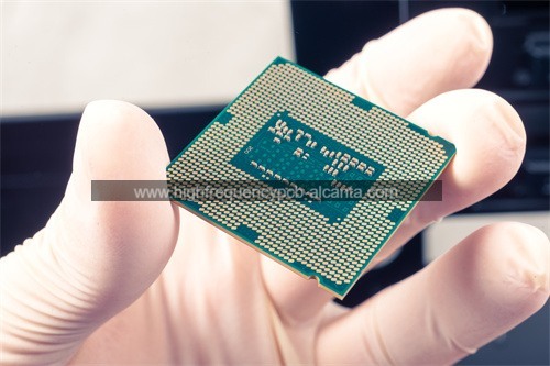
Ajinomoto(ABF) BGA Substrate Manufacturer
Ajinomoto(ABF) BGA Substrate Manufacturer,The Ajinomoto (ABF) BGA Substrate is a high-performance packaging material used in semiconductor devices. It incorporates Ajinomoto Build-up Film (ABF), a dielectric material known for its excellent electrical insulation and thermal stability. This substrate is essential for Ball Grid Array (BGA) packages, providing a reliable platform for mounting integrated circuits. The ABF BGA substrate supports fine pitch wiring, allowing for higher density interconnections and improved signal integrity. Its superior thermal properties ensure efficient heat dissipation, making it ideal for high-speed and high-power applications such as processors, memory modules, and advanced communication devices.
What is an Ajinomoto (ABF) BGA Substrate?
An Ajinomoto (ABF) BGA substrate is a high-performance substrate widely used in integrated circuit (IC) packaging. ABF stands for Ajinomoto Build-up Film, with Ajinomoto being a leading supplier of materials for this type of substrate, known for their advanced technology in high-density interconnect (HDI) and multilayer substrates.
The ABF BGA substrate uses a special resin material that boasts excellent electrical and mechanical properties. Its primary features include a low dielectric constant and low loss factor, ensuring superior signal integrity in high-frequency applications. Additionally, ABF material has excellent thermal and chemical stability, allowing the substrate to maintain good performance under high temperatures and environmental changes.
BGA (Ball Grid Array) is a packaging technology that connects the chip and the substrate using tiny solder balls. The ABF BGA substrate plays a crucial role in this packaging technology. It provides electrical connections and mechanical support and heat dissipation channels for the chip.
The manufacturing process of Ajinomoto ABF BGA substrates involves constructing multilayer structures and forming complex circuit patterns through lamination and drilling techniques. This multilayer structure supports high-density interconnects and fine lines, allowing the chip to have more pins and higher performance.
As electronic devices become increasingly miniaturized and functionally enhanced, ABF BGA substrates are becoming more widely used in high-performance computing, mobile devices, communication equipment, and consumer electronics. Their excellent material properties and advanced manufacturing techniques make them an indispensable part of modern high-density packaging technology.
Ajinomoto(ABF) BGA Substrate Manufacturer
What are the Ajinomoto (ABF) BGA Substrate Design Guidelines?
Ajinomoto (ABF) BGA substrate design guidelines are crucial for ensuring optimal performance and reliability of high-density interconnect (HDI) circuits. Here are the key design considerations:
- Material Selection: Use high-quality ABF materials that offer low dielectric constant and low dissipation factor to ensure excellent electrical performance and signal integrity. These materials are designed to handle high-frequency applications and thermal stress effectively.
- Layer Stacking: Carefully design the multilayer stack-up to achieve the required electrical performance and mechanical stability. Ensure proper alignment of layers and optimize layer thickness to balance performance and manufacturability.
- Trace and Pad Design: Design trace widths and pad sizes according to the current carrying capacity and impedance requirements. Use controlled impedance traces to maintain signal integrity and minimize signal loss and crosstalk.
- Via Design: Implement appropriate via structures to support high-density interconnects. Use microvias or blind/buried vias to minimize signal degradation and reduce parasitic inductance and capacitance.
- Thermal Management: Incorporate thermal vias and heat sinks to manage heat dissipation effectively. Proper thermal management ensures that the substrate and components remain within their operational temperature limits.
- Manufacturing Tolerances: Design with manufacturing tolerances in mind to ensure that the final product meets performance specifications. This includes considering aspects such as layer alignment, hole registration, and solder mask accuracy.
- Electrical Testing: Include design for testability features to facilitate electrical testing and debugging. Ensure that test points and access vias are provided for reliable testing of the substrate.
- Mechanical Considerations: Ensure the design accommodates mechanical stresses and strains that may occur during assembly and operation. Consider factors like warpage and flexural strength to maintain substrate integrity.
- Compliance with Standards: Adhere to industry standards and guidelines for BGA substrates, such as IPC standards for printed circuit boards and electronic assemblies. Compliance ensures reliability and compatibility with various components and systems.
- Reliability Testing: Conduct reliability testing, such as thermal cycling, moisture resistance, and mechanical shock tests, to validate the substrate’s performance under real-world conditions.
By following these design guidelines, you can optimize the performance and reliability of Ajinomoto (ABF) BGA substrates, ensuring they meet the demands of high-performance electronic applications.
What is the Ajinomoto (ABF) BGA Substrate Fabrication Process?
The Ajinomoto (ABF) BGA substrate fabrication process involves several key steps to produce high-quality substrates with advanced electrical and mechanical properties. Here’s an overview of the process:
- Material Preparation: Start with high-quality Ajinomoto Build-up Film (ABF) materials, which are specially formulated resin films with low dielectric constant and low dissipation factor. These materials provide the necessary electrical performance and thermal stability.
- Layer Lamination: Stack and laminate the ABF film layers to create the base structure of the substrate. The lamination process involves applying heat and pressure to bond the layers together, forming a multilayer structure with the desired thickness and layer configuration.
- Drilling and Via Formation: Drill holes in the laminated stack to create vias, which are used to connect different layers of the substrate. The vias can be through-hole, blind, or buried, depending on the design requirements. The drilling process must be precise to ensure accurate via alignment and dimensions.
- Electroplating and Metallization: Apply a thin layer of metal, typically copper, to the walls of the vias and the substrate surface. Electroplating is used to build up the metal layer, which forms the conductive paths for electrical connections. Metallization is crucial for ensuring reliable electrical performance and adhesion.
- Patterning and Etching: Use photolithography to apply a photoresist layer on the substrate surface. Expose the photoresist to UV light through a mask to define the circuit patterns. Then, etch away the unwanted copper to leave the desired circuit traces. This step is essential for creating the intricate circuitry required for high-density interconnects.
- Solder Mask Application: Apply a solder mask layer over the substrate to protect the circuit traces and prevent solder from bridging between different pads during assembly. The solder mask also defines the locations where solder will be applied for component mounting.
- Surface Finish: Apply a surface finish, such as electroless nickel immersion gold (ENIG) or immersion silver, to the exposed pads. The surface finish provides protection against oxidation and ensures good solderability during component assembly.
- Cutting and Shaping: Cut and shape the fabricated substrate to the required dimensions and form factors. This step includes trimming the edges and cutting the substrate into individual pieces or panels.
- Inspection and Testing: Perform thorough inspection and testing to ensure that the substrate meets all design specifications and quality standards. This includes electrical testing, visual inspection, and mechanical testing to check for defects or inconsistencies.
- Final Processing: Apply any additional processes, such as surface cleaning or coating, to prepare the substrate for final assembly. Ensure that the substrate is free of contaminants and ready for use in electronic packaging.
By following these fabrication steps, the Ajinomoto (ABF) BGA substrates are produced with high precision and reliability, meeting the demands of advanced electronic applications.
How do you manufacture an Ajinomoto (ABF) BGA Substrate?
Manufacturing an Ajinomoto (ABF) BGA substrate involves a series of precise and controlled steps to ensure high-quality performance and reliability. Here’s an overview of the manufacturing process:
- Material Preparation: Begin with high-quality Ajinomoto Build-up Film (ABF) resin, known for its low dielectric constant and low dissipation factor. These properties are crucial for high-frequency applications. The ABF film is prepared in rolls or sheets, ready for further processing.
- Layer Stacking and Lamination: Stack multiple layers of ABF film to create the base structure of the substrate. The layers are aligned and laminated together using heat and pressure to bond them into a solid multilayer structure. This step defines the substrate’s thickness and layer configuration.
- Drilling and Via Formation: Drill precise holes through the laminated stack to form vias, which will interconnect different layers of the substrate. This step requires high accuracy to ensure proper alignment and dimensions of the vias. The vias can be through-hole, blind, or buried based on the design.
- Electroplating and Metallization: Apply a thin layer of copper to the walls of the vias and the substrate’s surface through electroplating. This metal layer forms the conductive paths necessary for electrical connections. Metallization is essential for creating reliable and conductive pathways within the substrate.
- Patterning and Etching: Cover the substrate with a photoresist layer and use photolithography to define the circuit patterns. Expose the photoresist to UV light through a mask to transfer the circuit design. Then, etch away the excess copper to reveal the final circuit traces, creating the intricate patterns required for high-density interconnects.
- Solder Mask Application: Apply a solder mask layer over the substrate to protect the circuit traces and prevent solder from bridging between pads during component assembly. The solder mask also helps define the soldering areas for component attachment.
- Surface Finish Application: Apply a surface finish to the exposed pads, such as electroless nickel immersion gold (ENIG) or immersion silver. This finish protects the pads from oxidation and ensures good solderability, which is crucial for reliable component mounting.
- Cutting and Shaping:Trim and shape the substrate to the required dimensions and form factors. This includes cutting the substrate into individual panels or pieces, preparing them for final assembly and integration into electronic devices.
- Inspection and Testing: Conduct rigorous inspection and testing to verify that the substrate meets all design specifications and quality standards. This includes electrical testing to ensure proper functionality, visual inspection for defects, and mechanical testing for durability.
- Final Processing: Perform any additional processing required to prepare the substrate for its intended application. This may include cleaning, coating, or additional treatments to ensure that the substrate is ready for use in high-performance electronic assemblies.
By meticulously following these steps, manufacturers can produce Ajinomoto (ABF) BGA substrates that offer exceptional electrical performance, thermal stability, and mechanical reliability, meeting the demanding requirements of advanced electronic systems.
How much should an Ajinomoto (ABF) BGA Substrate cost?
The cost of an Ajinomoto (ABF) BGA substrate can vary widely based on several factors:
- Size and Complexity: Larger and more complex substrates, with intricate circuit patterns and multiple layers, generally cost more. The complexity of the design impacts the manufacturing time and material usage.
- Volume and Production Scale: Bulk production usually reduces the per-unit cost due to economies of scale. Higher volume orders often benefit from lower unit costs compared to smaller, custom orders.
- Material Specifications: The choice of ABF material type and grade can influence the cost. Higher-performance grades or custom formulations may be more expensive.
- Manufacturing Processes: Additional processes such as special surface finishes, advanced via structures (e.g., microvias), or enhanced thermal and electrical testing can increase the cost.
- Geographic Location: Manufacturing costs can vary by region due to differences in labor costs, material availability, and other local factors.
- Supplier and Market Conditions: Prices can fluctuate based on market demand, supplier pricing, and competition among manufacturers.
As a rough estimate, the cost of Ajinomoto (ABF) BGA substrates typically ranges from $10 to $100 per unit, depending on the aforementioned factors. For high-volume orders, the cost may be lower per unit, while custom or low-volume orders could be on the higher end of the range.
For a precise quote, it’s best to contact suppliers or manufacturers directly, providing details about the specific requirements and quantities needed.
What is Ajinomoto (ABF) BGA Substrate base material?
The base material for Ajinomoto (ABF) BGA substrates is Ajinomoto Build-up Film (ABF). This material is a type of epoxy resin film developed by Ajinomoto Co., Inc., specifically designed for high-performance electronic substrates. Here are some key characteristics of ABF base material:
- Low Dielectric Constant: ABF film has a low dielectric constant, which reduces signal loss and improves signal integrity, especially in high-frequency applications. This characteristic is crucial for high-speed and high-density electronic circuits.
- Low Dissipation Factor: The low dissipation factor of ABF film minimizes power loss and heat generation, which helps in maintaining performance and reliability over time.
- High Thermal Stability: ABF film can withstand high temperatures during the manufacturing process and in operation, ensuring stability and reliability under thermal stress.
- Good Chemical Resistance: The material is resistant to various chemicals and solvents used in the fabrication process, contributing to the durability and longevity of the substrate.
- High Mechanical Strength: ABF film provides good mechanical support and stability, essential for maintaining the integrity of fine traces and vias in high-density interconnect designs.
- Build-up Layer Capability: The film can be built up in multiple layers, allowing for complex and high-density circuit designs. This capability is particularly valuable in advanced BGA (Ball Grid Array) packages that require intricate layer structures.
In summary, Ajinomoto (ABF) BGA substrates use ABF film as their base material due to its excellent electrical, thermal, and mechanical properties, making it suitable for high-performance electronic applications.
Which company makes Ajinomoto (ABF) BGA Substrates?
Ajinomoto (ABF) BGA substrates are primarily manufactured by Ajinomoto Co., Inc., a leading supplier of ABF materials. Ajinomoto Co., Inc. specializes in developing and producing high-performance electronic materials, including ABF substrates for advanced packaging technologies. Due to its excellent electrical properties and thermal stability, ABF material is widely used in high-density interconnect (HDI) and high-frequency applications.
In addition to Ajinomoto Co., Inc., other companies in the market also manufacture similar ABF BGA substrates, but Ajinomoto remains the primary material supplier and technology provider.
Our company also manufactures Ajinomoto (ABF) BGA substrates. We have advanced manufacturing equipment and technology to provide high-quality ABF substrates that meet the stringent performance and reliability requirements of our customers. Here are our company’s production capabilities and advantages:
- Advanced Manufacturing Equipment: Our company is equipped with the latest manufacturing equipment, including high-precision laminators, drilling machines, electroplating, and etching equipment, ensuring high quality and consistency of the substrates.
- Professional Manufacturing Process: Our production processes include precise lamination, drilling, patterning, and surface treatment to produce high-performance ABF BGA substrates that meet international standards. We employ rigorous process control and quality inspection to ensure each substrate meets the expected performance requirements.
- Flexible Production Capabilities:Whether for large-scale production or small-batch customization, we can meet various customer needs. Our production lines can handle a wide range of specifications and complexities, allowing us to adapt to market changes and customer demands.
- High-Quality Material Supply:We use ABF materials from reputable suppliers, ensuring the electrical performance and thermal stability of the substrates. We also work with multiple material suppliers to ensure a stable supply of high-quality raw materials.
- Customer Support and Services: We provide comprehensive customer support, including technical consultation, design optimization advice, and after-sales service. Our team will work closely with customers to ensure that the products meet their needs and expectations.
In summary, our company can produce high-quality Ajinomoto (ABF) BGA substrates and is dedicated to providing excellent products and services to our customers. If you have any needs or questions, please feel free to contact us, and we will be happy to assist you.
What are the 7 qualities of good customer service?
Good customer service is crucial for building strong relationships with clients and ensuring their satisfaction. Here are seven key qualities of excellent customer service:
- Empathy: Understand and share the feelings of your customers. Show genuine concern for their issues and demonstrate that you care about their experience. Empathetic service helps in building trust and rapport, making customers feel valued and understood.
- Responsiveness: Provide prompt and effective responses to customer inquiries and issues. Quick resolution of problems and timely answers to questions show that you prioritize customer needs and respect their time.
- Professionalism: Maintain a high standard of professionalism in all interactions. This includes being polite, respectful, and knowledgeable. Professional service reflects positively on your company and builds credibility with customers.
- Communication Skills: Clearly and effectively communicate with customers. This involves active listening to understand their needs and providing clear, concise information. Good communication helps in preventing misunderstandings and ensures that customers are well-informed.
- Problem-Solving Abilities: Be proactive in addressing and resolving customer issues. Offer practical solutions and alternatives to meet their needs. Effective problem-solving demonstrates competency and helps in maintaining customer satisfaction.
- Patience: Exercise patience, especially when dealing with difficult or frustrated customers. Taking the time to listen and address their concerns calmly and thoroughly can help in diffusing tense situations and building a positive relationship.
- Follow-Up:Ensure that issues are fully resolved by following up with customers after the initial interaction. This shows commitment to customer satisfaction and helps in identifying any lingering concerns or additional needs.
By embodying these qualities, businesses can enhance their customer service, leading to increased customer satisfaction, loyalty, and positive word-of-mouth.
FAQs
What is the typical lead time for manufacturing Ajinomoto (ABF) BGA Substrates?
Lead times can vary depending on complexity and order volume, but typically range from 4 to 8 weeks.
Can Ajinomoto (ABF) BGA Substrates support high-frequency applications?
Yes, Ajinomoto (ABF) BGA Substrates are designed to support high-frequency applications with excellent signal integrity.
What are the common applications for Ajinomoto (ABF) BGA Substrates?
Common applications include advanced processors, memory modules, and other high-performance semiconductor devices.
How do you ensure the quality of Ajinomoto (ABF) BGA Substrates?
We ensure quality through rigorous testing, inspection, and adherence to industry standards.
Do you offer custom Ajinomoto (ABF) BGA Substrate designs?
Yes, we provide custom design services to meet specific requirements and applications.