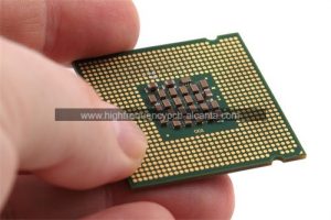
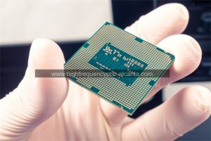
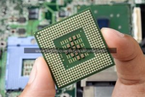
What is ABF Package Substrate?
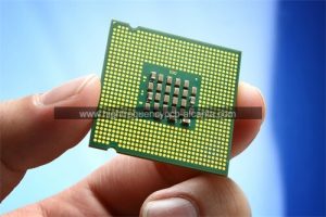
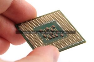
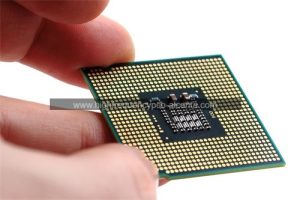
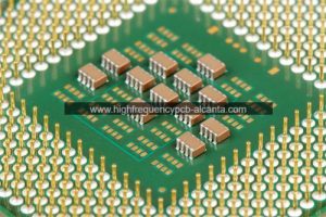
ABF Package substrate Manufacturer,ABF (Ajinomoto Build-up Film) package substrate is a cutting-edge material used in semiconductor packaging, featuring multiple layers of conductive traces and insulating materials. It enables precise and compact circuitry integration, reducing package size and enhancing electrical performance. ABF substrates ensure efficient heat dissipation, reliable electrical connections, and robust mechanical support, crucial for high-density applications like mobile devices and telecommunications equipment. With its advanced material composition and manufacturing techniques, ABF package substrates offer superior reliability, enabling the development of smaller, lighter, and more efficient electronic devices for various industries, from consumer electronics to automotive and beyond.
ABF Package substrate and Ro4350B packaging substrate manufacturer, high frequency BGA substrate, using the most advanced Sap process, Msap process technology, fast delivery, stable quality.
ABF, Ajinomoto Build-up Film, emerges as a sophisticated substrate material crucial in the domain of semiconductor packaging. Its primary function lies in providing a sturdy base for the mounting and interconnection of various electronic components within an integrated circuit (IC) package. Renowned for its superior thermal performance, reliability, and electrical characteristics, ABF substrates play a pivotal role in shaping the landscape of semiconductor technology.
Going beyond its foundational role, the package substrate assumes a critical function by establishing electrical connections between the IC and external environments like printed circuit boards (PCBs). Simultaneously, it actively contributes to dissipating the heat generated by semiconductor devices during their operational phases.
The adaptability of ABF substrates spans across avant-garde packaging technologies, encompassing innovations like flip-chip packaging and chip-on-film (COF) applications. Embracing these progressive packaging methodologies signifies a shared dedication to stretching technological limits, ultimately amplifying the holistic performance, downsizing, and dependability of electronic devices. Essentially, ABF substrates emerge as pivotal entities in the continuous transformation of semiconductor packaging approaches, proficiently addressing the ever-changing needs of the dynamic electronics industry.
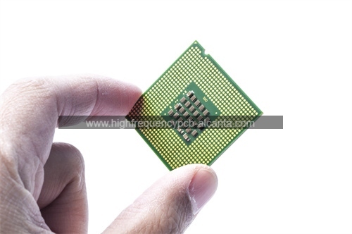
ABF package substrates
What is the Key Functionality of ABF Package Substrates?
At the heart of semiconductor innovation, ABF package substrates emerge as indispensable pillars, making a versatile impact on the functionality and reliability of electronic devices. Their fundamental role revolves around furnishing a resilient structural foundation, acting as the architectural backbone for the intricate amalgamation of varied electronic components within the confines of an integrated circuit (IC) package.
A pivotal function of these substrates lies in orchestrating seamless electrical interconnections among the various components of the integrated circuit. This involves creating conduits for the smooth transmission of signals, ensuring the harmonious operation and communication of the electronic device.
Renowned for their exceptional thermal performance, ABF substrates actively participate in the dissipation of heat generated during the operational phases of semiconductor devices. This dynamic heat management ensures optimal temperatures, mitigating the risk of overheating and sustaining the longevity of the electronic components.
Reliability is a hallmark attribute of ABF package substrates, ingrained in their meticulous material properties and design considerations. This steadfast reliability is instrumental in upholding the enduring stability and functionality of the integrated circuit, bolstering the overall dependability of electronic devices.
Beyond their foundational roles, ABF substrates take center stage in advanced packaging technologies. Embracing innovations like flip-chip packaging and chip-on-film (COF) applications, they propel the evolution of packaging methodologies. This commitment to cutting-edge techniques contributes significantly to enhancing performance, minimizing form factors, and elevating the reliability of electronic devices.
In essence, ABF package substrates are not just components; they are architectural keystones, intricately woven into the fabric of semiconductor technology, continuously evolving to meet the dynamic demands of the ever-changing electronic landscape.
What are the different types of ABF Package substrate?
ABF package substrates have been categorized into several types to address diverse needs in semiconductor packaging. However, keep in mind that specific types may have evolved or new categories may have emerged since then. Here are general classifications based on historical information:
Standard ABF Substrates:
These substrates form the traditional category, providing a baseline for electrical performance, thermal management, and reliability in standard semiconductor packaging applications.
High-Performance ABF Substrates:
Engineered to deliver superior electrical characteristics, enhanced thermal conductivity, and overall improved performance, these substrates are often chosen for advanced semiconductor applications where higher specifications are crucial.
Flip-Chip ABF Substrates:
Tailored for the specialized needs of flip-chip packaging technology, these substrates enable the direct connection of the active side of the semiconductor die to the substrate. This facilitates more compact designs and superior thermal efficiency.
COF (Chip-on-Film) ABF Substrates:
Specifically designed for chip-on-film applications, these substrates play a crucial role in flexible electronics. They allow semiconductor chips to be mounted directly on a thin film, providing flexibility for certain electronic components.
Customized ABF Substrates:
Manufacturers may produce ABF substrates with bespoke specifications based on the unique requirements of semiconductor devices or specific packaging technologies. Customization can involve adjustments in material composition, thickness, or other parameters to meet specific needs.
How Does ABF Package Substrate Differ from Traditional PCBs?
ABF (Ajinomoto Build-up Film) package substrates and traditional Printed Circuit Boards (PCBs) chart divergent paths in the intricate landscape of electronics.
Specialized Roles:
ABF Package Substrates: Precision-engineered to meet the specific demands of semiconductor packaging, ABF substrates act as the architectural linchpin for mounting and seamlessly connecting electronic components within integrated circuits (ICs).
Traditional PCBs: Embracing versatility, traditional PCBs serve as the workhorse for a myriad of electronic applications but lack the fine-tuned focus on the intricacies of semiconductor devices found in ABF substrates.
Material Symphony:
ABF Package Substrates: Crafted with advanced build-up films, ABF substrates boast a symphony of characteristics tailored to semiconductor tasks, including heightened thermal prowess and unwavering reliability.
Traditional PCBs: Comprising materials like FR-4, traditional PCBs offer a universal platform without the bespoke attributes intrinsic to ABF substrates.
Technological Choreography:
ABF Package Substrates: Dance at the forefront of advanced packaging technologies, including the nimble moves of flip-chip packaging and the graceful choreography of chip-on-film (COF) applications. Their steps align with the precision and miniaturization sought in modern semiconductor devices.
Traditional PCBs: While accommodating an array of electronic components, traditional PCBs may not harmonize as seamlessly with the intricate moves of cutting-edge packaging techniques prevalent in the semiconductor industry.
Integration Mastery:
ABF Package Substrates: Choreographed for a seamless pas de deux with semiconductor devices, ABF substrates ensure the precise electrical connections and graceful thermal management vital for the performance of ICs.
Traditional PCBs: While adept at facilitating electronic component mounting, traditional PCBs may not master the nuanced integration required for the grand performance of semiconductor devices.
In essence, ABF package substrates take center stage as specialized virtuosos, meticulously tuned to the demands of semiconductor packaging and avant-garde technologies. On the flip side, traditional PCBs provide a versatile ensemble, adept at harmonizing with a variety of electronic applications but lacking the bespoke notes crucial for the symphony of semiconductor devices.
What is the main structure and production technology of ABF package substrates?
The production technology and main structure of ABF (Ajinomoto Build-up Film) package substrates involve a series of intricate steps to create a robust foundation for semiconductor packaging. While specifics may vary among manufacturers, here’s a general overview:
Main Structure of ABF Package Substrates:
Base Material:ABF substrates commence with a base material, typically a thin film selected for its favorable electrical and thermal properties. This material forms the initial layer of the substrate.
Build-Up Layers:The distinctive feature of ABF substrates is the addition of build-up layers. Sequentially applied on top of the base material, these layers consist of dielectric materials and conductive traces. This layered approach forms a three-dimensional structure.
Copper Traces:Conductive traces, usually made of copper, are patterned on the dielectric layers. These traces serve as the essential electrical pathways, connecting various components within the integrated circuit (IC) package.
Dielectric Materials:Interspersed between the conductive traces, dielectric materials act as insulators. They contribute to the substrate’s electrical performance and provide necessary isolation between different layers.
Surface Finish:The topmost layer of the ABF substrate often undergoes a surface finish process. This may involve the application of protective coatings like solder mask to safeguard the substrate and provide a suitable surface for semiconductor device attachment.
Production Technology:
Film Lamination:The production process initiates with the lamination of thin films to establish the base material. This step involves the bonding of multiple layers to create a stable foundation.
Photolithography:Photolithography is employed to define the copper traces’ pattern on the dielectric layers. A photoresist is applied, exposed through a mask, and subsequently developed to form the desired copper trace pattern.
Etching:Exposed copper areas undergo an etching process, selectively removing unwanted material and leaving behind the intended conductive traces on the substrate.
Build-Up Process:The build-up process unfolds as dielectric layers and copper traces are meticulously added, creating the intricate three-dimensional structure. Each layer is carefully aligned and bonded to the existing substrate.
Surface Finish and Coating:The final layers receive surface finishes and protective coatings to enhance durability and shield the substrate from external factors.
Quality Control and Testing:Rigorous quality control measures and testing are implemented throughout the production process. These ensure that the substrate aligns with specified requirements for electrical performance, reliability, and other critical parameters.
It’s important to acknowledge that ABF package substrate production involves advanced manufacturing techniques. Continuous refinement and adaptation occur as manufacturers respond to the evolving demands within the semiconductor industry.
FAQs
What Defines ABF Package Substrates?
ABF package substrates stand as specialized materials integral to semiconductor packaging. They form the structural base for connecting and mounting electronic components within an integrated circuit (IC) package.
What Sets Apart the Characteristics of ABF Substrates?
Renowned for their superior thermal performance, reliability, and electrical attributes, ABF substrates are often the preferred choice in advanced packaging technologies, contributing to enhanced electronic device performance.
How Do ABF Substrates Differ from Traditional PCBs?
While ABF substrates target semiconductor packaging with a focus on ICs and advanced technologies, traditional PCBs offer versatility for a broader array of electronic applications.
Which Advanced Packaging Technologies Utilize ABF Substrates?
ABF substrates find their application in cutting-edge packaging technologies like flip-chip packaging and chip-on-film (COF). These advancements aim to elevate electronic device performance and reliability.
What Encompasses the Production Process of ABF Substrates?
The intricate production journey of ABF substrates includes steps such as film lamination, photolithography, etching, layer build-up, surface finishing, and rigorous quality control. This process shapes a structured substrate tailored for semiconductor packaging.
Where Can ABF Substrates Be Applied?
Predominantly used in semiconductor packaging, ABF substrates find their place in various electronic devices such as ICs, microprocessors, and memory components.
How Do ABF Substrates Contribute to Thermal Management?
ABF substrates actively contribute to thermal management by efficiently dissipating heat generated during semiconductor device operation. Their unique material properties and design considerations play a crucial role in maintaining optimal temperatures.
Is Customization Possible for ABF Substrates?
Absolutely, ABF substrates can be customized to meet specific requirements for semiconductor devices or packaging technologies. This flexibility may involve adjustments in material composition, thickness, and other parameters.
Conclusion
In summary, the incorporation of Advanced Buffer Materials (ABF) into package substrates signifies a substantial leap forward in the realm of PCB technology. As we bear witness to the constant evolution of electronic components, the role played by ABF becomes undeniably critical in elevating performance, ensuring reliability, and enhancing signal integrity within the intricate landscape of PCBs.
The specialized attributes of ABF substrates, notably their exceptional thermal performance and customized design tailored for semiconductor packaging, propel them into a key position in addressing the intricate demands of contemporary PCB technology.
The integration of ABF substrates is more than a mere structural enhancement; it represents a strategic response to the dynamic challenges posed by the ever-advancing field of electronic devices. Their application in sophisticated packaging technologies such as flip-chip packaging and chip-on-film (COF) applications underscores their adaptability and efficiency in meeting the evolving needs of the electronics industry.
In the face of electronic devices continually pushing the boundaries of innovation, the presence and influence of ABF in package substrates become indispensable. Its significance extends beyond providing structural support, actively contributing to the optimization of thermal management, electrical connectivity, and the overall reliability of integrated circuits. Thus, acknowledging the pivotal role of ABF in the broader context of PCB technology is imperative for embracing the continual advancements in the electronic landscape.
 Professional high frequency circuit board supplier
