 Professional high frequency circuit board supplier
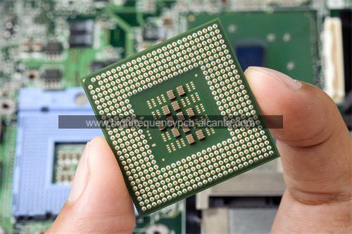
What is 3D IC Package Substrate?
3D IC Package Substrate Manufacturer,3D IC (Integrated Circuit) package substrate enables stacked semiconductor dies in a single package, enhancing performance and density. These substrates support vertical integration of chips, reducing interconnect length and improving signal speed. With advanced materials and precise manufacturing, 3D IC substrates ensure efficient heat dissipation and reliable electrical connections. Widely used in high-performance computing, AI, and data centers, they enable compact, high-density electronic assemblies with superior performance. 3D IC package substrates drive advancements in semiconductor packaging, enabling smaller form factors and higher processing power in electronic devices. Their innovative design and material properties empower the development of cutting-edge electronic systems.
A 3D IC package substrate, also known as a 3D integrated circuit package substrate, is a key component in three-dimensional integrated circuit (3D IC) packaging technology. In traditional integrated circuit (IC) packaging, chips are placed side by side on a single layer substrate. However, in 3D IC packaging, multiple layers of chips are stacked on top of each other, allowing for higher levels of integration, increased performance, and reduced form factor.
The 3D IC package substrate serves as a platform for connecting and interconnecting the stacked chips within the package. It provides electrical connections between the chips, as well as thermal management features to dissipate heat generated by the integrated circuits. The substrate typically consists of a multi-layered structure composed of various materials such as silicon, organic substrates (e.g., organic laminates), or glass interposers.
The design and fabrication of 3D IC package substrates require advanced technologies to ensure precise alignment, reliable electrical connections, and efficient thermal dissipation between the stacked chips. As 3D IC packaging continues to evolve, innovations in substrate materials, design techniques, and manufacturing processes are crucial for enabling the development of next-generation electronic devices with enhanced performance and functionality.
3D IC Package Substrate Manufacturer
What are the Functions of 3D IC Package Substrate?
The 3D IC package substrate serves several important functions in enabling the successful integration of multiple chips in a three-dimensional package. Some of the key functions include:
Electrical interconnection: The substrate provides the necessary electrical pathways for connecting the stacked chips within the package. It facilitates signal transmission, power distribution, and data exchange between the integrated circuits.
Signal integrity: The substrate helps to maintain signal integrity by minimizing signal loss, crosstalk, and other electrical interferences that can degrade the performance of the integrated circuits. Proper signal routing and impedance control are essential for ensuring reliable operation of the 3D IC package.
Thermal management: The substrate plays a crucial role in dissipating heat generated by the stacked chips during operation. It may incorporate features such as thermal vias, heat spreaders, and thermal planes to efficiently transfer heat away from the integrated circuits and prevent thermal issues such as overheating and thermal-induced stress.
Mechanical support and alignment: The substrate provides structural support for the stacked chips and ensures proper alignment and positioning within the package. It helps to maintain the integrity of the package assembly and prevents mechanical failures such as warpage and delamination.
Package integration and miniaturization: By enabling the stacking of multiple chips in a compact form factor, the 3D IC package substrate contributes to the miniaturization and integration of electronic devices. It allows for higher levels of functionality and performance in a smaller footprint, which is essential for applications requiring high-density packaging and space-constrained environments.
Overall, the functions of the 3D IC package substrate are critical for enabling the successful implementation of 3D IC packaging technology and unlocking the potential for enhanced performance, functionality, and efficiency in next-generation electronic devices.
What are the Different Types of 3D IC Package Substrate?
There are several different types of 3D IC package substrates, each with its own characteristics and advantages. Some common types include:
Silicon interposer: Silicon interposers are substrates made of silicon that provide a platform for connecting and interconnecting stacked chips within a 3D IC package. Silicon interposers offer high electrical performance, low signal loss, and excellent thermal conductivity, making them suitable for high-performance applications.
Organic interposer: Organic interposers are substrates made of organic materials such as organic laminates or build-up layers. They offer lower cost compared to silicon interposers and are suitable for applications where cost is a primary consideration. However, organic interposers may have lower electrical performance and thermal conductivity compared to silicon interposers.
Glass interposer: Glass interposers are substrates made of glass materials such as glass-ceramics or glass-reinforced substrates. They offer high thermal conductivity, excellent dimensional stability, and compatibility with high-density interconnect (HDI) technologies. Glass interposers are suitable for applications requiring high reliability and performance.
Through-silicon via (TSV) interposer: TSV interposers utilize through-silicon vias (TSVs) to provide vertical interconnections between stacked chips within a 3D IC package. TSV interposers offer high bandwidth, low latency, and compact form factor, making them suitable for high-speed and high-bandwidth applications such as memory stacking and advanced computing.
Ceramic interposer: Ceramic interposers are substrates made of ceramic materials such as alumina or aluminum nitride. They offer excellent thermal conductivity, mechanical strength, and reliability, making them suitable for applications requiring high-power dissipation and harsh operating environments.
These are just a few examples of the different types of 3D IC package substrates available. The choice of substrate type depends on various factors including performance requirements, cost considerations, and specific application needs. As 3D IC packaging technology continues to evolve, new substrate materials and designs are likely to emerge to address the demands of next-generation electronic devices.
How does 3D IC Package Substrate Relate to IC Packaging?
The 3D IC package substrate is a critical component of IC packaging, particularly in the context of advanced packaging technologies such as three-dimensional integrated circuit (3D IC) packaging. Here’s how it relates to IC packaging:
Integration of multiple chips: Traditional IC packaging typically involves placing individual chips side by side on a single layer substrate. In contrast, 3D IC packaging enables the stacking of multiple chips on top of each other, utilizing the 3D IC package substrate to provide interconnections between the stacked chips.
Electrical interconnection: The 3D IC package substrate facilitates electrical connections between the stacked chips within the package. It provides the necessary wiring and routing for signal transmission, power distribution, and data exchange between the integrated circuits.
Thermal management: Effective thermal management is crucial for maintaining the reliability and performance of integrated circuits. The 3D IC package substrate incorporates features such as thermal vias, heat spreaders, and thermal planes to dissipate heat generated by the stacked chips and prevent thermal issues such as overheating.
Signal integrity: Maintaining signal integrity is essential for ensuring reliable operation of the integrated circuits. The 3D IC package substrate is designed to minimize signal loss, crosstalk, and other electrical interferences that can degrade the performance of the package.
Mechanical support and alignment: The 3D IC package substrate provides structural support for the stacked chips and ensures proper alignment and positioning within the package. It helps to maintain the integrity of the package assembly and prevent mechanical failures such as warpage and delamination.
Overall, the 3D IC package substrate plays a crucial role in enabling the successful implementation of 3D IC packaging technology. It facilitates the integration of multiple chips in a compact form factor, while ensuring reliable electrical connections, efficient thermal management, and robust mechanical support. By leveraging advanced substrate materials, designs, and manufacturing processes, 3D IC packaging enables the development of next-generation electronic devices with enhanced performance, functionality, and miniaturization.
What are the Differences Between 3D IC Package Substrate and PCB?
The 3D IC package substrate and printed circuit board (PCB) serve different roles within electronic systems, although they share some similarities. Here are the key differences between the two:
Function and purpose:
3D IC package substrate: The primary purpose of a 3D IC package substrate is to provide a platform for integrating and interconnecting multiple chips within a three-dimensional package. It facilitates electrical connections, thermal management, and mechanical support for the stacked chips.
PCB: PCBs serve as the backbone of electronic systems, providing a platform for mounting and interconnecting various electronic components, including integrated circuits, resistors, capacitors, and connectors. PCBs facilitate electrical connections between components and provide mechanical support for the entire electronic system.
Integration level:
3D IC package substrate: 3D IC package substrates are typically used in advanced packaging technologies to integrate multiple chips within a single package. They enable high levels of integration and miniaturization by stacking chips vertically, which is not possible with traditional PCBs.
PCB: PCBs are used in conventional electronic systems to integrate and interconnect electronic components in a planar configuration. While PCBs can support moderate levels of integration, they are not designed for stacking chips vertically like 3D IC package substrates.
Material and construction:
3D IC package substrate: 3D IC package substrates are often made of materials such as silicon, organic laminates, glass interposers, or ceramic materials. They are designed specifically for high-density packaging applications and incorporate features such as through-silicon vias (TSVs), thermal management structures, and advanced interconnect technologies.
PCB: PCBs are typically constructed from laminates composed of fiberglass-reinforced epoxy resin with copper traces and layers of insulating material. PCBs can vary in complexity and construction depending on the specific application requirements but are generally less dense and sophisticated than 3D IC package substrates.
Application:
3D IC package substrate: 3D IC package substrates are used in advanced electronic devices requiring high levels of integration, performance, and miniaturization, such as high-end computing, networking, and mobile devices.
PCB: PCBs are used in a wide range of electronic devices and systems, including consumer electronics, automotive applications, industrial equipment, and telecommunications infrastructure.
In summary, while both 3D IC package substrates and PCBs play essential roles in electronic systems, they are designed for different applications and serve different functions. 3D IC package substrates are specialized components used for high-density packaging and vertical integration of chips, whereas PCBs are more general-purpose platforms for integrating and interconnecting electronic components in planar configurations.
What are the Main Structures and Production Technologies of 3D IC Package Substrate?
The main structures and production technologies of 3D IC package substrates can vary depending on factors such as substrate material, design requirements, and manufacturing processes. However, some common structures and production technologies include:
Silicon interposer:
Structure: Silicon interposers consist of a silicon wafer with multiple layers of metal interconnects and insulating layers. Through-silicon vias (TSVs) are used to provide vertical connections between the different layers.
Production technologies: Silicon interposers are typically fabricated using semiconductor manufacturing processes, including photolithography, etching, deposition, and bonding techniques. TSVs are created by etching holes through the silicon wafer and filling them with conductive material.
Organic interposer:
Structure: Organic interposers are composed of organic materials such as organic laminates or build-up layers. They may include multiple layers of conductive traces, dielectric layers, and vias for interconnection.
Production technologies: Organic interposers are manufactured using PCB fabrication techniques, including processes such as printing, etching, plating, and lamination. Advanced techniques such as laser drilling or mechanical drilling may be used to create vias in organic substrates.
Glass interposer:
Structure: Glass interposers are made of glass materials such as glass-ceramics or glass-reinforced substrates. They typically consist of multiple layers of glass with embedded conductive traces and vias.
Production technologies: Glass interposers are manufactured using glass processing techniques such as thin-film deposition, photolithography, etching, and bonding. Laser drilling or chemical etching may be used to create vias in glass substrates.
Ceramic interposer:
Structure: Ceramic interposers are composed of ceramic materials such as alumina or aluminum nitride. They consist of multiple layers of ceramic with embedded conductive traces and vias.
Production technologies: Ceramic interposers are fabricated using ceramic processing techniques such as tape casting, green machining, firing, and metallization. Laser drilling or punching may be used to create vias in ceramic substrates.
Through-silicon via (TSV) interposer:
Structure: TSV interposers utilize through-silicon vias (TSVs) to provide vertical connections between stacked chips. They typically consist of silicon wafers with TSVs and metal interconnects.
Production technologies: TSV interposers are manufactured using semiconductor fabrication processes similar to those used for silicon interposers, with a focus on TSV formation and integration.
Overall, the production technologies for 3D IC package substrates involve a combination of semiconductor manufacturing processes, PCB fabrication techniques, and specialized methods for creating vertical interconnections such as TSVs. These technologies enable the fabrication of complex substrate structures with high-density interconnects, thermal management features, and reliable electrical performance to meet the requirements of advanced packaging applications.
Frequently Asked Questions (FAQs):
What is a 3D IC package substrate?
A 3D IC package substrate is a critical component in three-dimensional integrated circuit (3D IC) packaging technology. It provides a platform for integrating and interconnecting multiple chips within a single package.
What are the functions of a 3D IC package substrate?
The functions of a 3D IC package substrate include electrical interconnection, thermal management, signal integrity, mechanical support, and package integration. It facilitates the integration of multiple chips, provides electrical connections between them, dissipates heat, ensures signal integrity, and supports the mechanical structure of the package.
What are the different types of 3D IC package substrates?
Common types of 3D IC package substrates include silicon interposers, organic interposers, glass interposers, ceramic interposers, and through-silicon via (TSV) interposers. Each type has its own characteristics and advantages, suited for different applications and requirements.
How does a 3D IC package substrate differ from a PCB?
While both serve as platforms for integrating and interconnecting electronic components, 3D IC package substrates are designed specifically for high-density packaging and vertical integration of chips, whereas PCBs are more general-purpose platforms for planar integration of components.
What are the main structures and production technologies of 3D IC package substrates?
The main structures of 3D IC package substrates include silicon, organic, glass, and ceramic interposers, as well as through-silicon via (TSV) interposers. Production technologies involve a combination of semiconductor manufacturing processes, PCB fabrication techniques, and specialized methods for creating vertical interconnections such as TSVs.
Conclusion
In conclusion, 3D IC package substrates play a crucial role in enabling the integration of multiple chips within a single package in advanced packaging technologies. They provide electrical interconnection, thermal management, signal integrity, mechanical support, and package integration, facilitating high levels of integration, performance, and miniaturization in electronic devices.
There are various types of 3D IC package substrates, including silicon, organic, glass, and ceramic interposers, as well as through-silicon via (TSV) interposers, each with its own characteristics and advantages. Production technologies involve a combination of semiconductor manufacturing processes, PCB fabrication techniques, and specialized methods for creating vertical interconnections such as TSVs.
Overall, 3D IC package substrates enable the development of next-generation electronic devices with enhanced performance, functionality, and efficiency, driving innovation in areas such as high-end computing, networking, mobile devices, and beyond. As technology continues to evolve, advancements in substrate materials, designs, and manufacturing processes will further push the boundaries of what is possible in electronic packaging.


