 Professional high frequency circuit board supplier
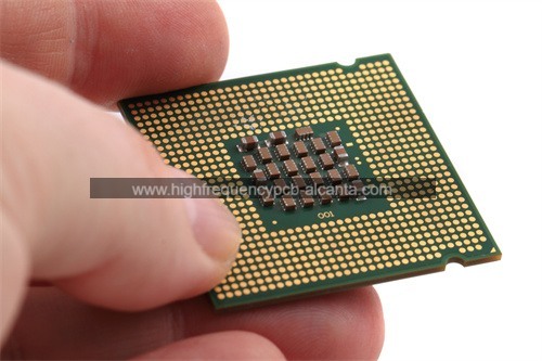
What is 2D IC Package Substrate?
2D IC Package Substrate Manufacturer,2D IC (Integrated Circuit) package substrate is a foundational platform for semiconductor packaging, supporting flat integration of chips. These substrates offer reliable electrical connections and mechanical support, ensuring stable performance in diverse applications. With precise routing and interconnect technologies, 2D IC substrates facilitate efficient signal transmission and thermal management. Commonly used in consumer electronics, automotive, and industrial applications, they enable the development of compact and efficient electronic assemblies. 2D IC package substrates drive advancements in semiconductor packaging, providing the backbone for a wide range of electronic devices. Their reliability and versatility make them indispensable for modern electronic systems requiring high performance and longevity.
A 2D IC package substrate refers to the substrate or board on which integrated circuits (ICs) are mounted in a two-dimensional arrangement. In the context of electronic packaging, a substrate is a base material onto which electronic components are mounted and interconnected. The term “2D IC package substrate” suggests that the integrated circuits are arranged in a flat, planar configuration on the substrate.
This type of substrate is commonly used in various electronic devices, including computers, smartphones, tablets, and other consumer electronics. The substrate provides mechanical support for the ICs and facilitates electrical connections between them and other components of the electronic system, such as memory modules, connectors, and input/output interfaces.
In summary, a 2D IC package substrate serves as a platform for mounting and interconnecting integrated circuits in a two-dimensional configuration within electronic devices.
2D IC Package Substrate Manufacturer
What are the Functions of 2D IC Package Substrate?
The 2D IC package substrate serves several important functions in electronic devices:
Mechanical Support: The substrate provides a stable platform for mounting and securing the integrated circuits (ICs) and other electronic components. It helps to protect the delicate ICs from physical damage due to handling, environmental factors, and mechanical stresses.
Electrical Interconnection: The substrate facilitates electrical connections between the ICs and other components within the electronic system. It typically contains conductive traces, vias, and pads that enable signal routing and power distribution between the ICs, as well as between the ICs and external interfaces such as connectors and sockets.
Thermal Management: The substrate helps dissipate heat generated by the ICs during operation. It may incorporate features such as thermal vias, metal layers, and heat spreaders to efficiently conduct heat away from the ICs and distribute it to thermal management components such as heat sinks or cooling fans.
Signal Integrity: The substrate plays a crucial role in maintaining signal integrity by minimizing signal loss, noise, and electromagnetic interference (EMI). Proper design and layout of the substrate’s conductive traces and signal paths help ensure reliable transmission of signals between the ICs and other components.
Component Integration: The substrate may incorporate additional passive components, such as capacitors, resistors, and inductors, to enhance the functionality of the electronic system or improve its performance. These components may be integrated directly into the substrate or mounted onto it using surface mount technology (SMT) or other assembly techniques.
Overall, the 2D IC package substrate is a critical component of electronic packaging that provides mechanical support, electrical interconnection, thermal management, signal integrity, and component integration for integrated circuits and other electronic components within electronic devices.
What are the Different Types of 2D IC Package Substrate?
There are several different types of 2D IC package substrates, each with its own characteristics and applications. Some common types include:
Printed Circuit Board (PCB): PCBs are perhaps the most widely used type of substrate in electronic packaging. They consist of a non-conductive material, typically fiberglass-reinforced epoxy, with conductive traces patterned on one or both sides. PCBs are suitable for a wide range of electronic applications and offer flexibility in terms of design, materials, and manufacturing processes.
Ceramic Substrate: Ceramic substrates are made from materials such as alumina (Al2O3) or aluminum nitride (AlN) and offer excellent thermal conductivity and mechanical strength. They are often used in high-power and high-frequency applications where thermal management and reliability are critical.
Flexible Substrate: Flexible substrates are made from thin, flexible materials such as polyimide or polyester. They are ideal for applications where space is limited or where the substrate needs to conform to a non-planar surface. Flexible substrates are commonly used in wearable electronics, flexible displays, and other portable devices.
Thick Film Substrate: Thick film substrates are made by depositing layers of ceramic paste onto a substrate material and then firing them at high temperatures to form thick film resistors, capacitors, and conductive traces. They are often used in hybrid integrated circuits (HICs) and other applications requiring integrated passive components.
Metal Core Substrate: Metal core substrates, also known as metal core printed circuit boards (MCPCBs), have a layer of metal (such as aluminum or copper) as the core material, providing excellent thermal conductivity. They are commonly used in high-power LED lighting applications and other applications requiring efficient thermal management.
Organic Substrate: Organic substrates are made from organic materials such as epoxy resin or polyimide. They offer good electrical properties, cost-effectiveness, and ease of manufacturing, making them suitable for a wide range of electronic applications.
These are just a few examples of the different types of 2D IC package substrates available. The choice of substrate type depends on various factors such as the specific application requirements, performance criteria, cost considerations, and manufacturing processes.
How does 2D IC Package Substrate Relate to IC Packaging?
2D IC package substrates are an integral component of IC packaging. They serve as the physical platform on which integrated circuits (ICs) are mounted and interconnected within electronic devices. The relationship between 2D IC package substrates and IC packaging is closely intertwined, as the substrate plays a crucial role in the overall performance, reliability, and functionality of the packaged ICs.
Here’s how 2D IC package substrates relate to IC packaging:
Mechanical Support: IC packaging involves encapsulating the semiconductor die (the actual IC) in a protective casing. The 2D IC package substrate provides a stable foundation for mounting and securing the packaged IC, ensuring mechanical stability and protection against physical damage.
Electrical Interconnection: IC packaging includes the routing of electrical connections between the semiconductor die and external components or interfaces. The 2D IC package substrate contains conductive traces, vias, and pads that facilitate electrical connections between the IC and other parts of the electronic system, such as connectors, sockets, and other ICs.
Thermal Management: Effective thermal management is essential for maintaining the reliability and performance of ICs. The 2D IC package substrate plays a crucial role in dissipating heat generated by the IC during operation, helping to regulate the temperature and prevent overheating. It may incorporate features such as thermal vias, metal layers, and heat spreaders to enhance thermal conductivity and heat dissipation.
Signal Integrity: Maintaining signal integrity is critical for ensuring reliable data transmission within electronic systems. The design and layout of the 2D IC package substrate influence signal integrity by minimizing signal loss, noise, and electromagnetic interference (EMI). Proper routing of signal traces and careful placement of components on the substrate help preserve signal quality and integrity.
Component Integration: In some cases, the 2D IC package substrate may integrate additional passive components, such as capacitors, resistors, and inductors, directly onto the substrate. This integration enhances the functionality and performance of the packaged IC and simplifies the overall system design.
In summary, the 2D IC package substrate is a critical element of IC packaging, providing mechanical support, electrical interconnection, thermal management, signal integrity, and sometimes component integration for the packaged ICs. Its design and characteristics significantly impact the overall performance, reliability, and functionality of electronic devices.
What are the Differences Between 2D IC Package Substrate and PCB?
While both 2D IC package substrates and printed circuit boards (PCBs) serve as platforms for mounting electronic components, there are several key differences between them:
Application and Functionality:
2D IC package substrates are specifically designed for mounting and interconnecting integrated circuits (ICs) within electronic devices. They are optimized for high-density packaging, signal integrity, and thermal management of ICs.
PCBs, on the other hand, have a broader range of applications and functionalities. They are used to mount various electronic components, including ICs, resistors, capacitors, connectors, and more. PCBs are often used for interconnecting components and providing structural support within electronic systems.
Material and Construction:
2D IC package substrates are typically constructed using specialized materials optimized for IC packaging, such as ceramic, organic substrates, or metal core substrates. These materials offer specific properties tailored to meet the requirements of IC packaging, such as thermal conductivity, mechanical strength, and signal integrity.
PCBs are commonly made from fiberglass-reinforced epoxy or other dielectric materials with conductive traces patterned on one or both sides. The choice of materials for PCBs depends on factors such as cost, mechanical properties, electrical performance, and manufacturing processes.
Integration of Components:
2D IC package substrates may integrate additional passive components, such as capacitors, resistors, and inductors, directly onto the substrate. This integration enhances the functionality and performance of the packaged ICs and simplifies system-level design.
While PCBs can also incorporate passive components, their primary function is to provide interconnection between various electronic components rather than serving as a platform for integrating components directly onto the substrate.
Design Complexity:
The design of 2D IC package substrates is typically more complex and specialized compared to PCBs. It involves considerations such as signal routing, thermal management, power distribution, and compatibility with specific IC packaging technologies.
PCB design can vary widely depending on the application and complexity of the electronic system but generally involves simpler layouts compared to 2D IC package substrates. PCB designs focus on optimizing signal routing, minimizing electromagnetic interference, and ensuring manufacturability and reliability.
In summary, while both 2D IC package substrates and PCBs serve as platforms for mounting electronic components, they differ in their application, construction, integration of components, and design complexity. 2D IC package substrates are specifically tailored for mounting and interconnecting ICs within electronic devices, whereas PCBs have a broader range of applications and functionalities.
What are the Main Structures and Production Technologies of 2D IC Package Substrate?
The main structures and production technologies of 2D IC package substrates can vary depending on the specific application requirements, materials used, and manufacturing processes. However, some common structures and production technologies include:
Structures:
Core Substrate: The core substrate forms the main structural foundation of the 2D IC package substrate. It is typically made of materials such as organic substrates (e.g., epoxy resin, polyimide), ceramic substrates (e.g., alumina, aluminum nitride), or metal core substrates (e.g., aluminum, copper). The core substrate provides mechanical support, electrical insulation, and thermal management for the integrated circuits.
Conductive Traces and Vias: Conductive traces and vias are patterns of metal (e.g., copper) that are deposited onto or embedded within the substrate material. These traces and vias form the electrical interconnections between the integrated circuits, passive components, and external interfaces. They are essential for routing signals, power, and ground connections within the substrate.
Dielectric Layers: Dielectric layers are insulating materials (e.g., resin, glass) that are sandwiched between conductive layers to provide electrical isolation and prevent short circuits. Dielectric layers are used to separate conductive traces, provide insulation between layers, and improve the overall reliability of the substrate.
Surface Finishes: Surface finishes are coatings applied to the substrate’s surface to enhance solderability, prevent oxidation, and improve the reliability of solder joints. Common surface finishes include electroless nickel immersion gold (ENIG), immersion silver (ImAg), and organic solderability preservatives (OSP).
Production Technologies:
Printed Circuit Board (PCB) Manufacturing: Many 2D IC package substrates are manufactured using standard PCB manufacturing processes, such as etching, drilling, plating, and solder mask application. PCB manufacturing involves several steps, including substrate preparation, conductive pattern formation, via drilling, plating, solder mask application, and surface finish.
Thin Film Deposition: Thin film deposition techniques, such as physical vapor deposition (PVD) and chemical vapor deposition (CVD), are used to deposit thin layers of metal or dielectric materials onto the substrate surface. Thin film deposition is often used to create conductive traces, dielectric layers, and surface finishes with precise thickness and composition.
Laser Ablation: Laser ablation is a precise manufacturing technique used to remove material from the substrate surface selectively. It is commonly used for drilling microvias and creating intricate patterns on the substrate surface with high accuracy.
Lamination: Lamination involves bonding multiple layers of substrate material together using heat and pressure. Lamination is used to create multilayer substrates with complex internal structures, such as buried vias, blind vias, and stacked vias.
These are some of the main structures and production technologies used in the manufacturing of 2D IC package substrates. The choice of structures and production technologies depends on factors such as substrate material, design complexity, performance requirements, and cost considerations.
Frequently Asked Questions (FAQs)
What is a 2D IC package substrate?
A 2D IC package substrate is a base material onto which integrated circuits (ICs) are mounted and interconnected in a two-dimensional arrangement within electronic devices.
What are the functions of a 2D IC package substrate?
The functions of a 2D IC package substrate include providing mechanical support for ICs, facilitating electrical interconnection between ICs and other components, managing thermal dissipation, preserving signal integrity, and sometimes integrating passive components.
What are the different types of 2D IC package substrates?
Common types of 2D IC package substrates include printed circuit boards (PCBs), ceramic substrates, flexible substrates, thick film substrates, metal core substrates, and organic substrates.
How does a 2D IC package substrate relate to IC packaging?
A 2D IC package substrate is an essential component of IC packaging, providing mechanical support, electrical interconnection, thermal management, signal integrity, and sometimes component integration for packaged ICs.
What are the main structures of a 2D IC package substrate?
The main structures of a 2D IC package substrate include the core substrate, conductive traces and pads, vias, and dielectric layers.
What are the production technologies used for 2D IC package substrates?
Production technologies for 2D IC package substrates may include traditional PCB manufacturing processes, thin film deposition, laser drilling, and additive manufacturing techniques.
What are the advantages of using 2D IC package substrates?
Advantages of using 2D IC package substrates include improved electrical performance, enhanced thermal management, increased design flexibility, and potential cost savings.
What factors should be considered when selecting a 2D IC package substrate?
Factors to consider when selecting a 2D IC package substrate include material properties, electrical performance, thermal conductivity, mechanical strength, design flexibility, cost, and manufacturability.
Conclusion
In conclusion, 2D IC package substrates play a critical role in electronic packaging by providing a platform for mounting and interconnecting integrated circuits (ICs) within electronic devices. These substrates offer mechanical support, facilitate electrical connections, manage thermal dissipation, preserve signal integrity, and sometimes integrate passive components to enhance functionality.
Various types of 2D IC package substrates exist, including printed circuit boards (PCBs), ceramic substrates, flexible substrates, thick film substrates, metal core substrates, and organic substrates. Each type has its own characteristics and production processes tailored to meet specific application requirements.
The production of 2D IC package substrates involves a combination of traditional PCB manufacturing processes, thin film deposition, laser drilling, and additive manufacturing techniques, allowing for customization and optimization of substrate properties.
Selecting the right 2D IC package substrate involves considering factors such as material properties, electrical performance, thermal conductivity, mechanical strength, design flexibility, cost, and manufacturability.
Overall, 2D IC package substrates contribute significantly to the performance, reliability, and functionality of electronic devices, making them an essential component of modern electronics packaging.


