 Professional high frequency circuit board supplier
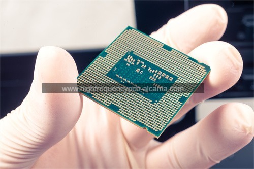
What is 2.5D IC Package Substrate?
2.5D IC Package Substrate Manufacturer,3D IC (Integrated Circuit) package substrate enables stacked semiconductor dies in a single package, enhancing performance and density. These substrates support vertical integration of chips, reducing interconnect length and improving signal speed. With advanced materials and precise manufacturing, 3D IC substrates ensure efficient heat dissipation and reliable electrical connections. Widely used in high-performance computing, AI, and data centers, they enable compact, high-density electronic assemblies with superior performance. 3D IC package substrates drive advancements in semiconductor packaging, enabling smaller form factors and higher processing power in electronic devices. Their innovative design and material properties empower the development of cutting-edge electronic systems.
A 2.5D IC (Integrated Circuit) package substrate is a type of advanced packaging technology used in semiconductor devices. In a 2.5D IC package, multiple chips, such as a processor and memory chips, are vertically stacked on top of each other, interconnected through an interposer or substrate.
The “2.5D” terminology refers to the fact that while the chips are stacked vertically, they are not directly stacked on top of each other like in a true 3D IC configuration, where individual layers of chips are interconnected through through-silicon vias (TSVs). Instead, the chips in a 2.5D configuration are interconnected through an interposer, which is a silicon or glass substrate that provides the electrical connections between the chips.
The use of a 2.5D IC package substrate offers several advantages, including improved performance, reduced power consumption, and smaller form factors compared to traditional packaging methods. It allows for higher levels of integration by enabling the assembly of heterogeneous chips (chips from different manufacturers or with different functionalities) into a single package, thus facilitating the development of more advanced and compact electronic devices.
2.5D IC Package Substrate Manufacturer
What are the Functions of 2.5D IC Package Substrate?
The 2.5D IC package substrate serves several essential functions in semiconductor devices. Some of the key functions include:
Interconnection: The substrate provides a platform for connecting multiple chips within the package. It enables the transmission of electrical signals, power, and data between the stacked chips.
Signal Routing: The substrate facilitates the routing of signals between the different chips, ensuring that data can be transmitted efficiently and reliably. This includes providing pathways for high-speed signals, such as those used for data communication between a processor and memory chips.
Power Distribution: The substrate distributes power to the various components within the package, ensuring that each chip receives the necessary power supply for operation. It also manages power integrity, minimizing voltage drops and noise to maintain stable power delivery.
Thermal Management: The substrate helps dissipate heat generated by the stacked chips, ensuring that the temperature remains within acceptable limits. This can involve incorporating thermal vias or other structures to conduct heat away from the chips and to the package’s exterior for dissipation.
Mechanical Support: The substrate provides structural support for the stacked chips, helping to ensure the reliability and durability of the package. It also helps to protect the chips from mechanical stress and environmental factors.
Integration of Heterogeneous Components: The substrate enables the integration of heterogeneous components, allowing chips from different manufacturers or with different functionalities to be stacked together in a single package. This facilitates the development of advanced, highly integrated electronic systems.
Overall, the 2.5D IC package substrate plays a crucial role in enabling the integration, connectivity, and performance of semiconductor devices with stacked chip configurations.
What are the Different Types of 2.5D IC Package Substrate?
There are several different types of 2.5D IC package substrates, each with its own characteristics and advantages. Some of the common types include:
Silicon Interposer: Silicon interposers are widely used in 2.5D IC packaging. These substrates are typically made from silicon wafers and feature a network of metal traces and through-silicon vias (TSVs) for interconnecting the stacked chips. Silicon interposers offer excellent electrical performance, low signal loss, and high bandwidth, making them suitable for high-performance applications.
Glass Interposer: Glass interposers are an alternative to silicon interposers. They are made from glass substrates and utilize similar interconnection techniques, such as metal traces and TSVs. Glass interposers offer advantages such as lower cost, larger panel sizes, and better thermal properties compared to silicon interposers.
Organic Interposer: Organic interposers are made from organic materials, such as laminate substrates or build-up substrates. These substrates offer lower cost and better scalability compared to silicon and glass interposers. However, they may have limitations in terms of electrical performance and thermal management.
Fan-Out Wafer-Level Packaging (FO-WLP): FO-WLP is a packaging technology that involves redistributing the I/Os (input/output) of a chip to a larger area on the same wafer or to multiple wafers. While not strictly a 2.5D IC package substrate, FO-WLP can be considered a form of advanced packaging that enables the integration of multiple chips within a single package.
Embedded Die Interposer: Embedded die interposers involve embedding one or more chips within the substrate material itself. This approach can offer advantages in terms of size reduction, improved electrical performance, and enhanced thermal management.
These are just a few examples of the types of 2.5D IC package substrates available. The choice of substrate depends on factors such as performance requirements, cost considerations, and the specific needs of the application.
How does 2.5D IC Package Substrate Relate to IC Packaging?
2.5D IC package substrate is a specific type of advanced packaging technology that is closely related to traditional IC packaging but offers additional capabilities and advantages. Here’s how 2.5D IC package substrate relates to IC packaging:
Integration of Multiple Chips: Traditional IC packaging typically involves packaging a single chip (integrated circuit) into a package. In contrast, 2.5D IC package substrates allow for the integration of multiple chips within a single package. These chips can include different types of ICs, such as processors, memory, and specialized accelerators, stacked on top of each other and interconnected through the substrate.
Interconnection: Both traditional IC packaging and 2.5D IC package substrates involve interconnecting the chip’s I/Os (input/output) to the external environment. However, in 2.5D IC packaging, the interconnection is more complex due to the presence of multiple stacked chips. The substrate facilitates the electrical connections between these chips, enabling them to communicate with each other and with external devices.
Performance Enhancement: 2.5D IC package substrates offer advantages in terms of performance enhancement compared to traditional IC packaging. By stacking multiple chips together, the distance between them is reduced, leading to shorter interconnect lengths and lower parasitic capacitance and resistance. This results in improved signal integrity, higher bandwidth, and lower power consumption.
Heterogeneous Integration: 2.5D IC package substrates enable heterogeneous integration, allowing chips from different manufacturers or with different functionalities to be integrated into a single package. This facilitates the development of more advanced and specialized systems-on-chip (SoCs) with enhanced capabilities and performance.
Thermal Management: In both traditional IC packaging and 2.5D IC package substrates, thermal management is essential to ensure the reliability and longevity of the packaged devices. However, in 2.5D IC packaging, the presence of multiple stacked chips can lead to higher heat dissipation requirements. The substrate plays a crucial role in facilitating effective heat dissipation and thermal management strategies.
Overall, while 2.5D IC package substrates share some similarities with traditional IC packaging, they offer additional capabilities and advantages that enable more advanced and integrated semiconductor devices.
What are the Differences Between 2.5D IC Package Substrate and PCB?
2.5D IC package substrates and printed circuit boards (PCBs) are both essential components in electronic systems, but they serve different purposes and have distinct characteristics. Here are some key differences between 2.5D IC package substrates and PCBs:
Functionality:
2.5D IC Package Substrate: The primary function of a 2.5D IC package substrate is to provide a platform for interconnecting and stacking multiple chips within a single package. It facilitates high-density integration, heterogeneous integration, and advanced packaging techniques such as through-silicon vias (TSVs) and interposers.
PCB: PCBs serve as the backbone of electronic systems, providing mechanical support and electrical connections for various electronic components such as integrated circuits (ICs), resistors, capacitors, and connectors. PCBs are typically used for mounting and interconnecting components in electronic devices.
Interconnection Density:
2.5D IC Package Substrate: 2.5D IC package substrates typically have higher interconnection density compared to PCBs. They are designed to accommodate the complex interconnections between multiple stacked chips, often utilizing advanced packaging technologies such as TSVs, microbumps, and fine-pitch interconnects.
PCB: While PCBs can also support high-density interconnections, they are generally not as dense as 2.5D IC package substrates. PCBs typically have larger feature sizes and wider spacing between traces, limiting their interconnection density compared to advanced packaging substrates.
Integration Level:
2.5D IC Package Substrate: 2.5D IC package substrates enable high levels of integration by allowing multiple chips to be stacked vertically within a single package. This facilitates the integration of heterogeneous components and enables the development of more compact and advanced electronic systems.
PCB: While PCBs can support integration to some extent, they are primarily used for integrating discrete electronic components and connecting them together. PCBs are typically used in systems where components are mounted side by side rather than stacked vertically.
Manufacturing Complexity:
2.5D IC Package Substrate: Manufacturing 2.5D IC package substrates involves advanced semiconductor fabrication processes, such as lithography, etching, deposition, and wafer bonding. These processes are complex and require specialized equipment and expertise.
PCB: PCB manufacturing involves processes such as PCB layout design, etching, drilling, and soldering. While PCB manufacturing also requires expertise, it is generally less complex compared to manufacturing 2.5D IC package substrates.
Overall, while both 2.5D IC package substrates and PCBs are essential components in electronic systems, they serve different purposes and have distinct characteristics in terms of functionality, interconnection density, integration level, and manufacturing complexity.
What are the Main Structures and Production Technologies of 2.5D IC Package Substrate?
The main structures and production technologies of 2.5D IC package substrates vary depending on the specific type of substrate and manufacturing processes used. However, some common structures and production technologies include:
Interposer or Substrate Material: The substrate material is typically a silicon, glass, or organic substrate. Silicon interposers offer excellent electrical performance and high bandwidth but can be expensive to manufacture. Glass interposers provide lower cost and better thermal properties but may have limitations in electrical performance. Organic interposers offer lower cost and better scalability but may have lower electrical performance and thermal conductivity.
Metal Traces: Metal traces are patterned on the substrate to provide electrical interconnections between the stacked chips. These traces carry signals, power, and data between the chips within the package.
Through-Silicon Vias (TSVs): TSVs are vertical interconnects that pass through the substrate, connecting the metal traces on different layers. TSVs are commonly used in silicon interposers to enable high-density interconnections and reduce signal path lengths.
Build-Up Layers: Build-up layers are additional layers of dielectric material deposited on the substrate to create a multilayered structure. These layers provide isolation between metal traces and enable complex routing of signals within the substrate.
Bump Formation: Bumps or microbumps are fabricated on the substrate to provide electrical connections between the substrate and the stacked chips. These bumps are typically made of solder or copper and are placed on the substrate’s surface in a predefined pattern.
Wafer-Level Processing: Some 2.5D IC package substrates are manufactured using wafer-level processing techniques, where multiple substrates are processed simultaneously on a wafer. This enables high throughput and cost-effective production of substrates.
Die Bonding and Stacking: After the substrates are fabricated, the chips are bonded to the substrate using die attach techniques. The chips are then stacked on top of each other and bonded together using methods such as solder reflow or thermocompression bonding.
Interconnection and Packaging: Once the chips are stacked and bonded, the package undergoes interconnection processes to establish electrical connections between the chips and external devices. This may involve wire bonding, flip-chip bonding, or other interconnection techniques.
These are just some of the main structures and production technologies used in the fabrication of 2.5D IC package substrates. The specific processes and materials can vary depending on factors such as performance requirements, cost considerations, and the desired characteristics of the final package.
Frequently Asked Questions (FAQs)
What is a 2.5D IC package substrate?
A 2.5D IC package substrate is a type of advanced packaging technology used in semiconductor devices. It involves stacking multiple chips on top of each other and interconnecting them through a substrate or interposer.
What are the functions of a 2.5D IC package substrate?
The functions of a 2.5D IC package substrate include interconnection of stacked chips, signal routing, power distribution, thermal management, mechanical support, and integration of heterogeneous components.
What are the different types of 2.5D IC package substrates?
Common types of 2.5D IC package substrates include silicon interposers, glass interposers, organic interposers, embedded die interposers, and fan-out wafer-level packaging (FO-WLP).
How does a 2.5D IC package substrate relate to IC packaging?
A 2.5D IC package substrate is a type of IC packaging technology that enables the integration of multiple chips within a single package. It offers advantages such as improved performance, smaller form factors, and heterogeneous integration compared to traditional IC packaging.
What are the main structures and production technologies of 2.5D IC package substrates?
Main structures and production technologies include interposer or substrate material selection (e.g., silicon, glass, organic), metal traces, through-silicon vias (TSVs), build-up layers, bump formation, wafer-level processing, die bonding and stacking, and interconnection and packaging.
Conclusion
In conclusion, 2.5D IC package substrates represent an advanced packaging technology that enables the integration of multiple chips within a single package. These substrates offer numerous benefits, including improved performance, smaller form factors, and heterogeneous integration compared to traditional IC packaging methods. By stacking chips vertically and interconnecting them through substrates or interposers, 2.5D IC package substrates facilitate the development of highly integrated semiconductor devices with enhanced capabilities. The main structures and production technologies of these substrates vary, but they typically involve selecting appropriate materials, fabricating metal traces and through-silicon vias, creating build-up layers, forming bumps for interconnection, and employing wafer-level processing and die bonding techniques. Overall, 2.5D IC package substrates play a crucial role in advancing semiconductor technology and enabling the development of next-generation electronic devices.


