

ABF Package Substrate Manufacturer
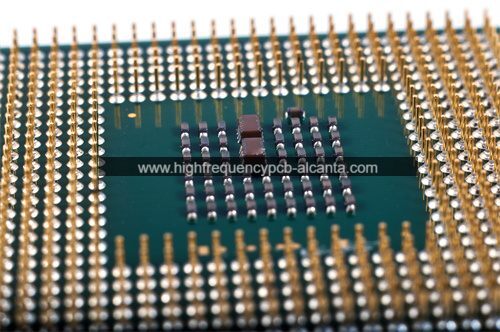
ABF Package Substrate Manufacturer,ABF (Ajinomoto Build-up Film) Package Substrates are advanced printed circuit boards characterized by their use of build-up film technology. These substrates feature multiple layers of insulating material with embedded conductive traces, allowing for dense interconnects and fine-pitch component placement. ABF Package Substrates excel in high-density packaging applications where space efficiency and signal integrity are crucial, such as mobile devices, computing systems, and high-speed communication equipment. They are designed to minimize signal loss and support high-frequency operation, ensuring stable performance in demanding environments. ABF Package Substrates are preferred for their superior thermal and mechanical properties, contributing to the miniaturization and efficiency of modern electronic designs.
What is an ABF Package Substrate Manufacturer?
An ABF (Ajinomoto Build-up Film) Package Substrate Manufacturer specializes in producing substrates used in advanced packaging technologies for integrated circuits (ICs). ABF substrates are known for their high-density interconnects, which enable efficient signal transmission and thermal management in electronic devices. These manufacturers employ specialized processes to build multilayered structures using ABF films, creating platforms that support the mounting and interconnection of semiconductor chips. These substrates are crucial in modern electronics, facilitating miniaturization, improved performance, and reliability in a variety of applications from consumer electronics to telecommunications infrastructure. Companies in this field often focus on innovation in materials, manufacturing techniques, and design to meet the evolving demands of the semiconductor industry.
ABF Package Substrate Manufacturer
What are the ABF Package Substrate Design Guidelines?
The design guidelines for ABF (Ajinomoto Build-up Film) Package Substrates generally include several key considerations to ensure optimal performance and reliability:
- Layer Stackup Design:Designing the appropriate number of layers and their configuration to meet signal integrity and power delivery requirements.
- Material Selection: Choosing ABF films and other materials based on thermal management, electrical properties, and compatibility with assembly processes.
- Routing and Signal Integrity: Ensuring controlled impedance for high-speed signals, minimizing crosstalk, and optimizing signal paths to maintain signal integrity.
- Thermal Management: Incorporating thermal vias and considerations for heat dissipation to prevent overheating of components.
- Via Design:Proper placement and size of vias to facilitate efficient electrical connections and thermal management without compromising reliability.
- Alignment and Registration: Ensuring precise alignment during manufacturing processes to maintain alignment accuracy of layers and components.
- Manufacturing Tolerances: Designing with consideration for manufacturing capabilities and tolerances to ensure consistent production quality.
- Reliability and Testing: Incorporating design features that facilitate testing and reliability assessments during manufacturing and after deployment.
- Environmental Considerations: Designing for resistance to environmental factors such as moisture, humidity, and temperature variations.
- Compliance and Standards: Ensuring compliance with industry standards and specifications relevant to ABF substrates and their applications.
These guidelines help ensure that ABF Package Substrates meet performance, reliability, and manufacturability requirements for a wide range of electronic applications.
What is the ABF Package Substrate Fabrication Process?
The fabrication process of ABF (Ajinomoto Build-up Film) Package Substrates typically involves several key steps:
- Substrate Preparation: The process begins with preparing a base substrate, often made of materials like FR-4 or other suitable substrates, which serve as the foundation for building the ABF layers.
- Build-up Layer Formation: ABF films, which are typically polyimide-based films with conductive and insulating layers, are laminated onto the base substrate. These films provide the structural foundation for creating the multilayered circuitry.
- Laser Drilling and Via Formation: Laser drilling or mechanical drilling processes create vias through the ABF layers. Vias are essential for establishing electrical connections between different layers of the substrate.
- Copper Plating and Circuit Patterning: After drilling, the vias are plated with copper to create conductive pathways. Circuit patterns are then formed using photolithography and etching processes to define the conductive traces and pads on each layer.
- Dielectric Layer Deposition: Additional layers of dielectric material may be deposited to insulate and separate conductive traces, ensuring electrical isolation and preventing short circuits.
- Surface Finish and Coating: Surface finishes such as solder mask and final coatings are applied to protect the substrate, provide solderability, and facilitate component assembly.
- Quality Control and Testing: Throughout the fabrication process, various quality control measures are employed to ensure the integrity and reliability of the substrate. Testing may include checks for dimensional accuracy, electrical continuity, impedance control, and thermal performance.
- Final Inspection and Packaging: Once fabrication is complete, substrates undergo final inspection to verify compliance with specifications and standards. They are then packaged and prepared for shipment to customers or assembly facilities.
The ABF Package Substrate fabrication process is complex and requires precise control over materials, processes, and quality assurance to meet the stringent requirements of modern electronics applications.
How do you manufacture ABF Package Substrates?
Manufacturing ABF (Ajinomoto Build-up Film) Package Substrates involves a detailed process to ensure high-performance and reliability:
- Substrate Preparation: Begin with a base substrate, often FR-4 or similar material, which provides structural support.
- Build-up Layer Formation: Laminate ABF films onto the base substrate. These films consist of polyimide layers with conductive and insulating properties.
- Drilling and Via Formation: Use laser or mechanical drilling to create vias through the ABF layers. Vias establish electrical connections between substrate layers.
- Copper Plating and Circuit Patterning: Plate vias with copper to form conductive pathways. Define circuit patterns via photolithography and etching for traces and pads.
- Dielectric Layer Deposition: Deposit additional dielectric layers to insulate and separate conductive traces, preventing short circuits.
- Surface Finish and Coating: Apply solder mask and protective coatings to ensure substrate integrity and facilitate soldering during component assembly.
- Quality Control: Implement rigorous testing throughout fabrication. Ensure dimensional accuracy, electrical continuity, impedance control, and thermal performance.
- Final Inspection and Packaging: Conduct comprehensive inspections to verify compliance with specifications. Package substrates for shipment to customers or assembly facilities.
Manufacturers of ABF Package Substrates adhere to strict processes and quality standards to meet the demands of diverse electronic applications, ensuring durability, performance, and reliability.
How much should an ABF Package Substrate Manufacturer cost?
The cost of ABF (Ajinomoto Build-up Film) Package Substrates can vary significantly based on several factors:
- Design Complexity: More complex designs with multiple layers, fine-pitched features, and specific material requirements can increase costs due to higher manufacturing complexity.
- Material Costs: ABF films and other materials used in substrate fabrication contribute to overall costs. High-performance materials and specialized coatings may incur higher expenses.
- Manufacturing Volume: Larger production volumes often lead to economies of scale, reducing per-unit costs. Small production runs or prototypes may be more expensive per unit.
- Technology and Equipment: Advanced manufacturing technologies and equipment required for precise drilling, plating, and layer deposition influence manufacturing costs.
- Quality and Certification: Compliance with industry standards and certifications may affect costs, as additional testing and quality assurance processes can add to overall expenses.
- Supplier Relationships: Relationships with material suppliers and subcontractors can impact costs, especially if there are fluctuations in material prices or availability.
- Geographical Location: Manufacturing costs can vary based on the location of the manufacturer, labor costs, and overhead expenses.
To get a specific cost estimate for ABF Package Substrates, it’s advisable to contact manufacturers directly with detailed specifications and volume requirements. They can provide quotations tailored to the specific needs of the project, considering factors such as design complexity, materials, and production volume.
What is ABF Package Substrate Base Material?
The base material used in ABF (Ajinomoto Build-up Film) Package Substrates typically refers to the underlying substrate onto which the ABF films are applied and processed. Common base materials include:
- FR-4:A widely used epoxy-based laminate substrate known for its electrical insulation properties and mechanical stability. It provides a solid foundation for building multilayered substrates.
- BT (Bismaleimide Triazine): Known for its excellent thermal stability and low dielectric constant, BT substrates are suitable for high-frequency applications and those requiring superior thermal management.
- Ceramic Substrates:Such as LTCC (Low Temperature Co-fired Ceramic) or HTCC (High Temperature Co-fired Ceramic), which offer excellent thermal conductivity, mechanical strength, and reliability in harsh environments.
These base materials are chosen based on the specific requirements of the application, including electrical performance, thermal management needs, dimensional stability, and compatibility with the ABF build-up process. Each material has its advantages and is selected to optimize the performance and reliability of the final ABF Package Substrate.
Which companies manufacture ABF Package Substrates?
Several companies manufacture ABF (Ajinomoto Build-up Film) Package Substrates. Some major manufacturers include Ajinomoto Fine-Techno from Japan, a pioneer in ABF technology offering a range of ABF substrates for high-density interconnects and thermal management solutions. Another prominent manufacturer is Shin-Etsu Chemical, also based in Japan, with extensive experience and technology in ABF substrates. Additionally, Ryosan Company, Ltd. from Taiwan and Samsung Electro-Mechanics from South Korea are significant suppliers, providing high-quality products and custom solutions in the ABF substrate market.
Our company is also capable of producing ABF Package Substrates. We specialize in using advanced manufacturing technologies and high-quality materials to offer customized solutions to our customers. With a professional design team and precision production equipment, we can meet various complex design requirements and high-performance application needs. Whether it’s high-density interconnects, intricate circuit layouts, or stringent quality control, we ensure product stability and reliability. Our production processes adhere to international standards, ensuring each batch of products meets customer requirements and expectations.
If you have any inquiries regarding ABF Package Substrates or would like to learn more about our company’s capabilities and products, please feel free to contact us. We are committed to providing the best solutions for our customers and contributing to the success of your projects.
What are the 7 qualities of good customer service?
The 7 qualities of good customer service are:
- Responsiveness: Being prompt in addressing customer inquiries, issues, and requests. Customers appreciate quick responses and efficient resolution of their concerns.
- Empathy: Understanding and showing empathy towards customers’ perspectives, feelings, and situations. Empathetic communication helps build rapport and trust.
- Clarity: Providing clear and concise information to customers. Effective communication ensures that customers understand the information and instructions provided.
- Patience: Demonstrating patience, especially when dealing with challenging situations or customers. Patient interactions contribute to a positive customer experience.
- Knowledge:Possessing in-depth knowledge about products, services, and policies. Well-informed staff can offer accurate guidance and solutions to customers.
- Professionalism: Maintaining professionalism in conduct and communication. Professional behavior instills confidence in customers regarding the company’s reliability and competence.
- Personalization: Tailoring interactions and solutions to meet individual customer needs. Personalized service makes customers feel valued and enhances satisfaction.
These qualities collectively contribute to creating a positive customer service experience, fostering customer loyalty, and promoting business growth.
FAQs
What are ABF Package Substrates?
ABF Package Substrates are advanced circuit board substrates made using Ajinomoto Build-up Film technology. They are known for their high-density interconnects and thermal management capabilities.
What are the advantages of ABF Package Substrates?
ABF substrates offer advantages such as high reliability, excellent thermal performance, and the ability to support complex circuit designs with fine-pitched features.
What applications are ABF Package Substrates used in?
They are used in various applications including telecommunications, automotive electronics, consumer electronics, and industrial equipment where high reliability and performance are critical.
How are ABF Package Substrates manufactured?
The manufacturing process involves laminating ABF films onto base substrates, drilling vias, copper plating, circuit patterning, dielectric layer deposition, and surface finishing to create multilayered substrates.
What factors should be considered when choosing ABF Package Substrates?
Considerations include design complexity, thermal management requirements, electrical performance, reliability standards, and cost-effectiveness for the specific application.
Which companies manufacture ABF Package Substrates?
Major manufacturers include Ajinomoto Fine-Techno, Shin-Etsu Chemical, and other leading electronics companies known for their expertise in ABF technology.
How can I ensure the quality of ABF Package Substrates?
Ensuring quality involves selecting reputable manufacturers, adhering to industry standards, conducting rigorous testing, and verifying compliance with specifications during production.